Light-emitting diode and its manufacturing method
A technology of light-emitting diodes and light-emitting layers, which is applied in the manufacturing of semiconductor/solid-state devices, semiconductor devices, electrical components, etc., can solve the problems affecting the luminous purity and recombination efficiency of light-emitting devices, and affect the luminous performance of quantum dots, and improve the luminous purity of devices. , to avoid parasitic luminescence, the method is simple and easy to control the effect
- Summary
- Abstract
- Description
- Claims
- Application Information
AI Technical Summary
Problems solved by technology
Method used
Image

Examples
preparation example Construction
[0047] Correspondingly, another aspect of the embodiments of the present invention provides a method for manufacturing a light-emitting diode, and the method includes the following steps:
[0048] providing a substrate on which an anode is prepared;
[0049] Depositing a double heterojunction nanorod material on the anode to prepare a first light-emitting layer; depositing a quantum dot light-emitting material on the first light-emitting layer to prepare a second light-emitting layer;
[0050] preparing a cathode on said second emissive layer; or
[0051] The preparation method comprises the following steps:
[0052] providing a substrate on which a cathode is prepared;
[0053] Depositing a quantum dot luminescent material on the cathode to prepare a second luminescent layer; depositing a double heterojunction nanorod material on the second luminescent layer to prepare a first luminescent layer;
[0054] An anode is prepared on the first light-emitting layer.
[0055] The...
Embodiment approach
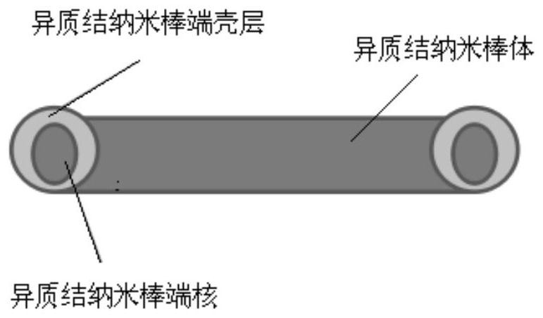
[0059] In particular, the double heterojunction nanorod material in the embodiment of the present invention contains double heterojunction nanorods, and the double heterojunction nanorods include nanorod bodies, and nanorod ends connecting the two ends of the nanorod bodies , and the nanorod end is a core-shell structure, and the core-shell structure includes a nanorod end core and a nanorod end shell covering the surface of the nanorod end core. A represents the nanorod material, B represents the nanorod end core material, and C represents the nanorod end shell material. As a preferred embodiment, the preparation method of the double heterojunction nanorod includes the following steps:
[0060] (1) A / B nanorod precursor is prepared, and the A / B nanorod precursor refers to that the nanorod body material is A, the nanorod end core material is B, and the nanorod end core is connected to the nanorod body two ends nanorod structure.
[0061] Preferably, the A / B nanorod precursor ...
Embodiment 1
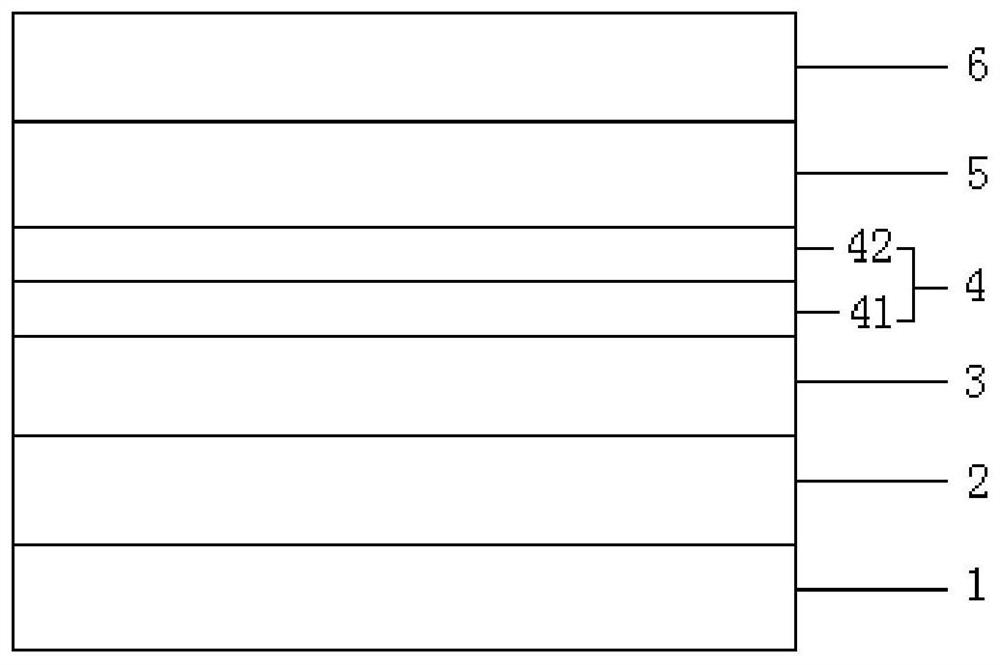
[0068] A light-emitting diode, including an anode and a cathode arranged oppositely, the anode is arranged on a glass substrate, a double-layer light-emitting layer is arranged between the anode and the cathode, and a double-layer light-emitting layer is arranged between the anode and the double-layer A hole functional layer between the light-emitting layers, an electron functional layer disposed between the cathode and the double-layer light-emitting layer, wherein the double-layer light-emitting layer includes a first light-emitting layer adjacent to the anode and an adjacent The second light-emitting layer provided on the cathode, the hole functional layer includes a hole injection layer and a hole transport layer sequentially arranged on the anode, and the electron functional layer is an electron transport layer. In the above light-emitting diodes, the anode material is ITO, the hole injection layer material is PEDOT:PSS, the hole transport layer material is TFB, the first ...
PUM
| Property | Measurement | Unit |
|---|---|---|
| thickness | aaaaa | aaaaa |
| luminescence spectroscopy | aaaaa | aaaaa |
| luminescence spectroscopy | aaaaa | aaaaa |
Abstract
Description
Claims
Application Information
 - Generate Ideas
- Intellectual Property
- Life Sciences
- Materials
- Tech Scout
- Unparalleled Data Quality
- Higher Quality Content
- 60% Fewer Hallucinations
Browse by: Latest US Patents, China's latest patents, Technical Efficacy Thesaurus, Application Domain, Technology Topic, Popular Technical Reports.
© 2025 PatSnap. All rights reserved.Legal|Privacy policy|Modern Slavery Act Transparency Statement|Sitemap|About US| Contact US: help@patsnap.com