Light emitting device and manufacturing method thereof

A light-emitting device and quantum dot light-emitting technology, which is applied in the manufacture of semiconductor/solid-state devices, electric solid-state devices, semiconductor devices, etc., can solve the problems of unbalanced electron and hole transport rates, and achieve the promotion of electron and hole transport balance, The effect of slowing down the decline of materials and prolonging the working life

Active Publication Date: 2022-05-31
TCL CORPORATION
View PDF7 Cites 0 Cited by
  • Summary
  • Abstract
  • Description
  • Claims
  • Application Information

AI Technical Summary

Problems solved by technology

[0004] The purpose of the present invention is to provide a method for preparing a light-emitting device, aiming to solve the technical problem of unbalanced transport rates of electrons and holes in existing light-emitting devices to a certain extent

Method used


Image

  • Light emitting device and manufacturing method thereof
  • Light emitting device and manufacturing method thereof
  • Light emitting device and manufacturing method thereof

Examples


preparation example Construction

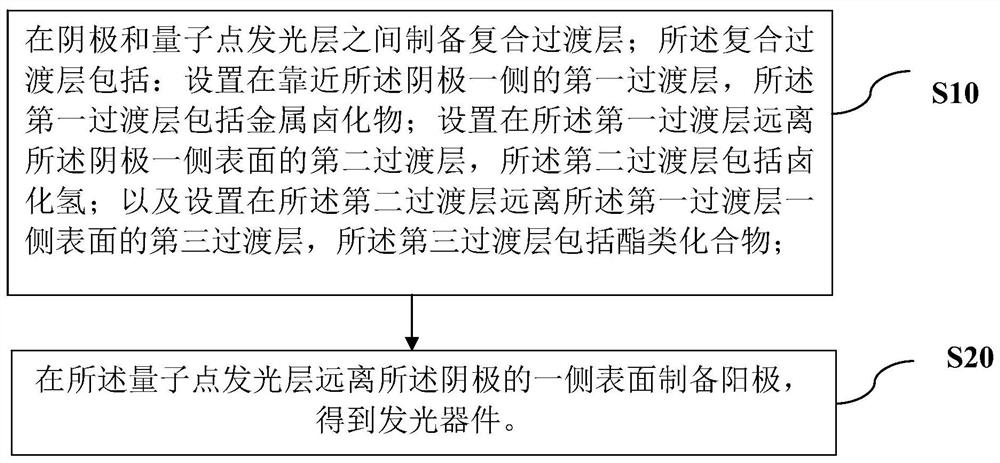
[0021] S20. Prepare an anode on the surface of the quantum dot light-emitting layer away from the cathode to obtain a light-emitting device.

[0026] S12. Prepare a hole functional layer between the quantum dot light-emitting layer and the anode;

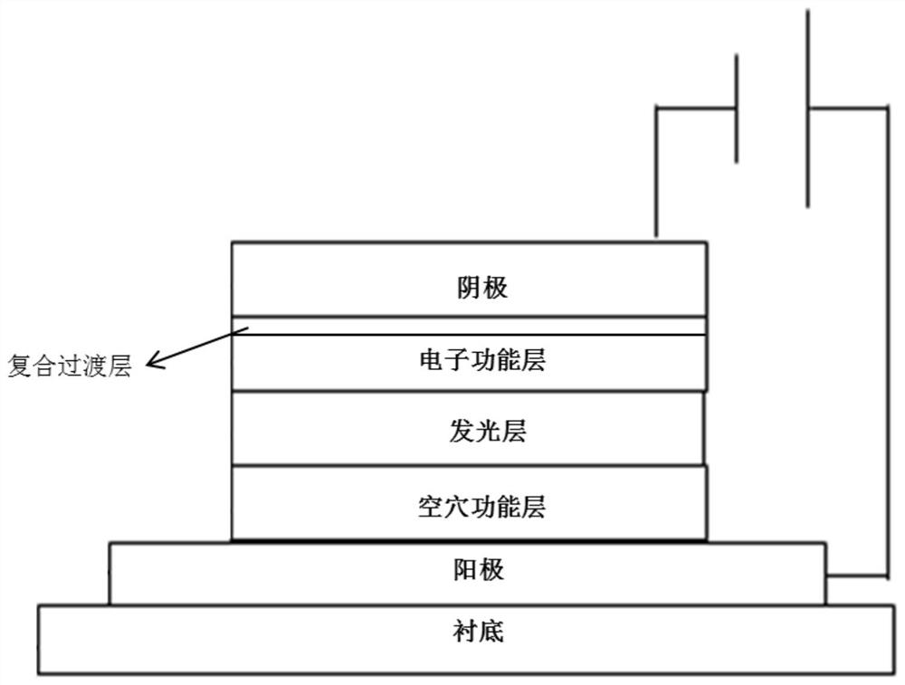
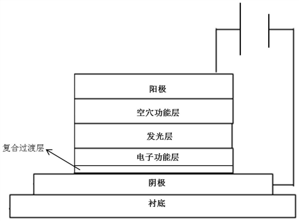
[0028] Specifically, in the above-mentioned step S10, a composite transition layer is set between the cathode and the quantum dot light-emitting layer. the present invention

[0045] In some embodiments, the concentration of the acid halide compound solution is 5-20 mg / mL. If the acid halide compound dissolves

[0046] In some embodiments, the metal element in the metal halide is the same as the metal element in the metal cathode.

[0047] In some embodiments, the thickness of the composite transition layer is 10-20 nanometers. In some specific embodiments, the

[0051] In some embodiments, the thickness of the composite transition layer is 10-20 nanometers. In some specific embodiments, the

[0052] In some embodiments, the cathode ...

Embodiment 1

[0073] Step S14: on the quantum dot light-emitting layer, deposit an ethanol solution of zinc oxide nanomaterials, pre-anneal at 80 ° C for 5 min, remove

[0076] Step S17: annealing at 80° C. for 30 minutes, encapsulating and curing, and completing the preparation of the quantum dot light-emitting device.

Embodiment 2

[0082] Step S24: on the quantum dot light-emitting layer, depositing an ethanol solution of zinc oxide nanomaterials, pre-annealing at 80° C. for 5 min, removing

[0085] Step S27: annealing at 80° C. for 30 minutes, encapsulating and curing, and completing the preparation of the quantum dot light-emitting device.


PUM

PropertyMeasurementUnit
thicknessaaaaaaaaaa
thicknessaaaaaaaaaa
thicknessaaaaaaaaaa

Abstract

The invention belongs to the technical field of display devices, and in particular relates to a method for preparing a light-emitting device, comprising the steps of: preparing a composite transition layer between a cathode and a quantum dot light-emitting layer; the composite transition layer includes: a first transition layer, the first transition layer includes a metal halide; a second transition layer disposed on the surface of the first transition layer away from the cathode side, the second transition layer includes hydrogen halide; and The third transition layer on the surface of the second transition layer away from the first transition layer, the third transition layer includes an ester compound; prepared on the surface of the quantum dot light-emitting layer away from the cathode anode to obtain a light-emitting device.

Description

Light-emitting device and preparation method thereof technical field [0001] The present invention belongs to the technical field of display devices, in particular to a light-emitting device and a preparation method thereof. Background technique [0002] Quantum dot electroluminescence is a new type of solid-state lighting technology, with low cost, light weight, fast response speed, It has the advantages of high color saturation and broad development prospects, and has become one of the important research directions of the new generation of LED display devices. one. The light-emitting diode QLED based on semiconductor quantum dots has better monochromaticity, color saturation and lower Due to the advantages of equipment cost and other advantages, it shows broad application prospects in the field of display and lighting. After rapid development in recent years, its luminous Key performance indicators such as brightness, external quantum efficiency (EQE) and lifetime h...

Claims


Application Information

Patent Timeline
Patent Type & Authority Patents(China)
IPC IPC(8): H01L51/50H01L51/56
CPCH10K30/865H10K50/115H10K50/16H10K71/00Y02P70/50H10K50/171H10K2102/351H10K71/15H10K50/15
Inventor 宋音洁张建新杨一行
Owner TCL CORPORATION
Why Eureka
Try Eureka