Display panel and preparation method thereof
A display panel and longitudinal cross-section technology, applied in semiconductor/solid-state device manufacturing, electrical components, electrical solid-state devices, etc., can solve the problems of color shift and impure luminescence, and achieve the effect of preventing color shift and improving luminous purity.
- Summary
- Abstract
- Description
- Claims
- Application Information
AI Technical Summary
Problems solved by technology
Method used
Image

Examples
Embodiment 1
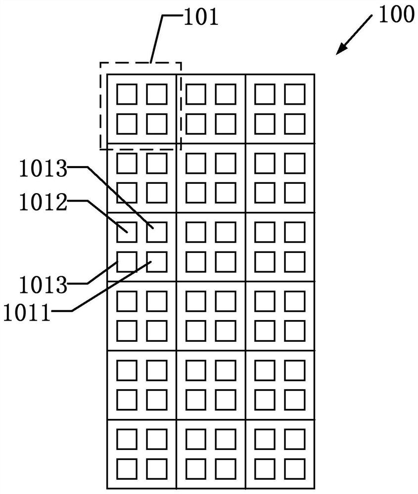
[0046] Such as figure 1 , figure 2As shown, this embodiment provides a display panel 100 . The display panel 100 includes a plurality of pixel units 101 arranged in an array. Each pixel unit 101 includes a plurality of sub-pixels. In this embodiment, each pixel unit 101 includes: a first sub-pixel 1011 , a second sub-pixel 1012 and two third sub-pixels 1013 . More preferably, in this embodiment, the first sub-pixel 1011 is a red sub-pixel, the second sub-pixel 1012 is a blue sub-pixel, and the third sub-pixel 1013 is a green sub-pixel. Wherein, the first sub-pixel 1011 is located at the lower right corner of the pixel unit 101, the second sub-pixel 1012 is located at the upper left corner of the pixel unit 101, and the two third sub-pixels 1013 are respectively located at the pixel unit 101 the lower left and upper right corners of the . In other embodiments, the colors of the first sub-pixel 1011, the second sub-pixel 1012, and the third sub-pixel 1013 can be replaced a...
Embodiment 2
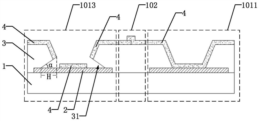
[0062] Such as Figure 8 As shown, this embodiment includes most of the technical features of Embodiment 1, and its difference from Embodiment 1 is that the third sub-pixel 1013 of Embodiment 2 is close to the pixel blocking unit of the first sub-pixel 1011 A first notch 31 is formed in the middle of the side wall. In this embodiment, the longitudinal cross-sectional shape of the first notch 31 is triangular, and the first notch 31 has an included angle α, and the included angle α is less than or equal to 20°. The depth of the first notch 31 thus formed is relatively deep, which can ensure the gap between the functional layer 4 on the surface of the anode unit 2 and the functional layer 4 on the surface of the pixel barrier unit 3 provided with the first notch 31 when the functional layer 4 is prepared. There is a gap, which prevents the lateral conduction between the third sub-pixel 1013 and the first sub-pixel 1011, thereby preventing the first sub-pixel 1011 from being lit...
Embodiment 3
[0065] Such as Figure 13 As shown, this embodiment includes most of the technical features of Embodiment 1. The difference between this embodiment and Embodiment 1 is that the third sub-pixel 1013 is close to the side of the pixel blocking unit 3 of the second sub-pixel 1012 The wall is provided with a second notch 34 . At this time, the length of the first gap 31 is smaller than the length of the third sub-pixel 1013 ; the length of the second gap 34 is smaller than the width of the third sub-pixel 1013 . Specifically, the length of the first gap 31 is shorter than the opening length L1 of the third sub-pixel 1013 ; the length of the second gap 34 is smaller than the opening width L2 of the third sub-pixel 1013 . In this way, the four corners of the third sub-pixel 1013 can be retained, ensuring that the cathode prepared later is continuous.
PUM
 Abstract
Description
Claims
Application Information
 - Generate Ideas
- Intellectual Property
- Life Sciences
- Materials
- Tech Scout
- Unparalleled Data Quality
- Higher Quality Content
- 60% Fewer Hallucinations
Browse by: Latest US Patents, China's latest patents, Technical Efficacy Thesaurus, Application Domain, Technology Topic, Popular Technical Reports.
© 2025 PatSnap. All rights reserved.Legal|Privacy policy|Modern Slavery Act Transparency Statement|Sitemap|About US| Contact US: help@patsnap.com