
Method for parallelly detecting synchronous communication chips

A test method and technology of communication chips, which are applied in the direction of electronic circuit testing, measuring electricity, measuring devices, etc., can solve the problems of probe pollution, poor test, probe oxidation, etc., so as to shorten the test time, reduce the test cost, and reduce the test time. the effect of shortening

Active Publication Date: 2007-06-13
SHANGHAI HUAHONG GRACE SEMICON MFG CORP
View PDF0 Cites 13 Cited by
  • Summary
  • Abstract
  • Description
  • Claims
  • Application Information

AI Technical Summary

Problems solved by technology

Because too many needle sticks will pollute the probe and easily oxidize the probe, so too many needle sticks will cause poor test problems

Method used


Image

  • Method for parallelly detecting synchronous communication chips
  • Method for parallelly detecting synchronous communication chips

Examples


Embodiment Construction

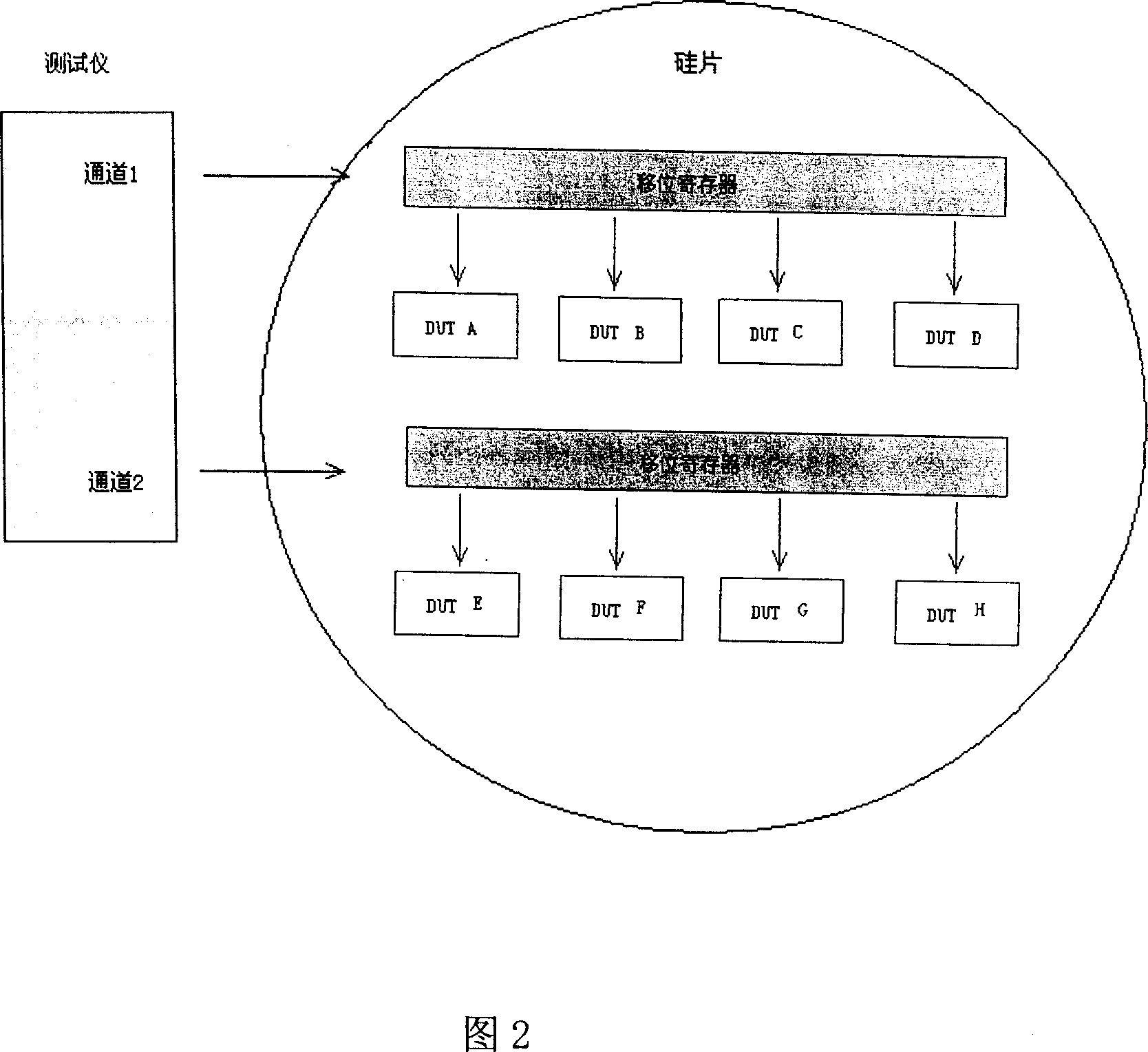
[0009] Boundary scan is a relatively advanced test method, which connects various modules in the chip through the shift register for testing, so as to realize the controllability and observability of the test. The present invention adopts the method of boundary scanning to test a plurality of synchronous communication chips in parallel, which can effectively improve the test efficiency.

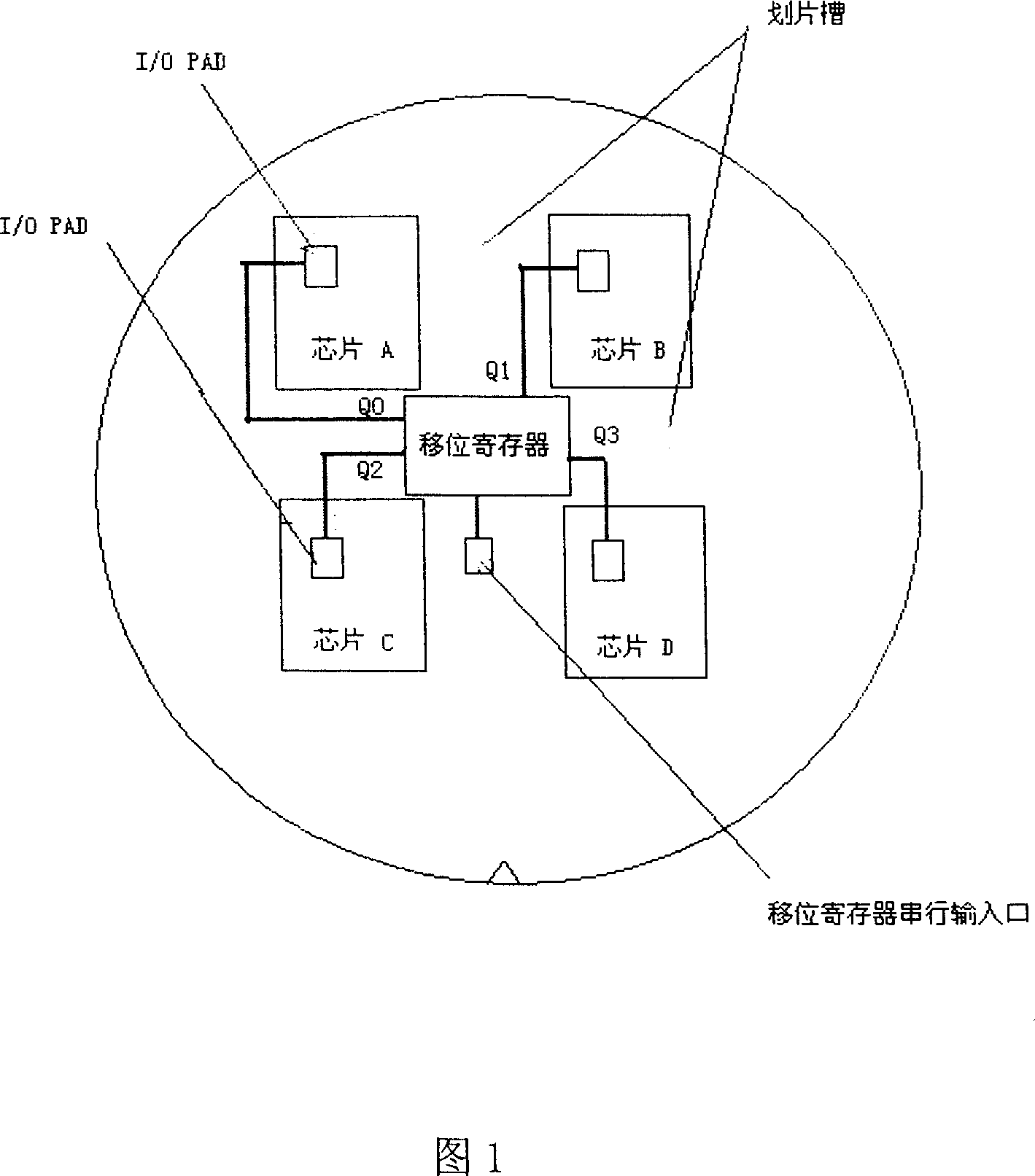
[0010] The parallel testing method of the synchronous communication chip of the present invention regards a plurality of chips on a silicon chip as a plurality of modules on a chip, and uses parallel ports on a shift register to connect to the plurality of chips. The specific solution is: as shown in Figure 1, on the same silicon chip, a four-bit bidirectional input-output shift register is made on the scribe slot, and the parallel output port of the shift register is connected to the PAD ( Pressure point) on the signal terminal (such as I / O PAD), pierce the probe of the tester to the serial ...


PUM


Abstract

The invention discloses a method to take multi-chip parallel testing by using synchronous communication chip. It includes the following steps: connecting plural chips on silicon slice by shift register, outputting the testing signal to tested chips by the method of series to parallel, inputting the output data to I / O pins of tester from plural chips by the method of parallel to series, and reading the data and taking data process to gain the PASS / FAIL result of the chips. The invention could improve testing efficiency of testing chip and lower testing time and cost.

Description

technical field [0001] The invention relates to a large-scale integrated circuit testing method, in particular to a method for parallel testing multiple large-scale integrated circuit synchronous communication chips. Background technique [0002] With the development of large-scale integrated circuits, the circuit becomes more and more complex, and the required test time becomes longer and longer. In order to save the test time, it is necessary to increase the number of simultaneous tests for parallel testing of multiple chips. At the same time, as the critical dimensions used in semiconductor manufacturing are getting smaller and smaller, the number of chips on the same silicon wafer is also increasing. This not only increases the test time, but also increases the number of needle sticks on the probe station. Because too many needle sticks will pollute the probe and easily oxidize the probe, so too many needle sticks will cause poor testing. Contents of the invention ...

Claims


Application Information

Patent Timeline
IPC IPC(8): G01R31/28G01R31/00
Inventor 武建宏
Owner SHANGHAI HUAHONG GRACE SEMICON MFG CORP
Learn More