Self-emission panel and method of manufacturing the same

A manufacturing method and self-illumination technology, applied in electroluminescent light sources, semiconductor/solid-state device manufacturing, light sources, etc., can solve the problems of reduced productivity, hindrance to the miniaturization/lightweight of electronic equipment, and rising costs

Inactive Publication Date: 2007-06-06
TOHOKU PIONEER CORP
View PDF1 Cites 4 Cited by
  • Summary
  • Abstract
  • Description
  • Claims
  • Application Information

AI Technical Summary

Problems solved by technology

Therefore, in the periphery of the wiring lead-out part and driver IC mounting part that do not require a large area, a redundant area is formed like part A of Figure 1 (b), and the number that can be obtained relative to the area of ​​the mother supporting substrate is reduced, becoming a potential problem. The reason for the increase in cost and the increase in the occupied area of ​​​​the self-luminous panel alone has the problem of hindering the miniaturization / lightweight of electronic equipment equipped with self-luminous panels
[0008] In addition, although it is also considered to cut the mother support substrate into a complicated shape to reduce the unnecessary area, when cutting into a complicated shape, cracks are likely to occur at the corners, and there is a possibility that the productivity will be lowered due to the deterioration of the yield. The problem

Method used


Image

  • Self-emission panel and method of manufacturing the same
  • Self-emission panel and method of manufacturing the same
  • Self-emission panel and method of manufacturing the same

Examples


Embodiment Construction

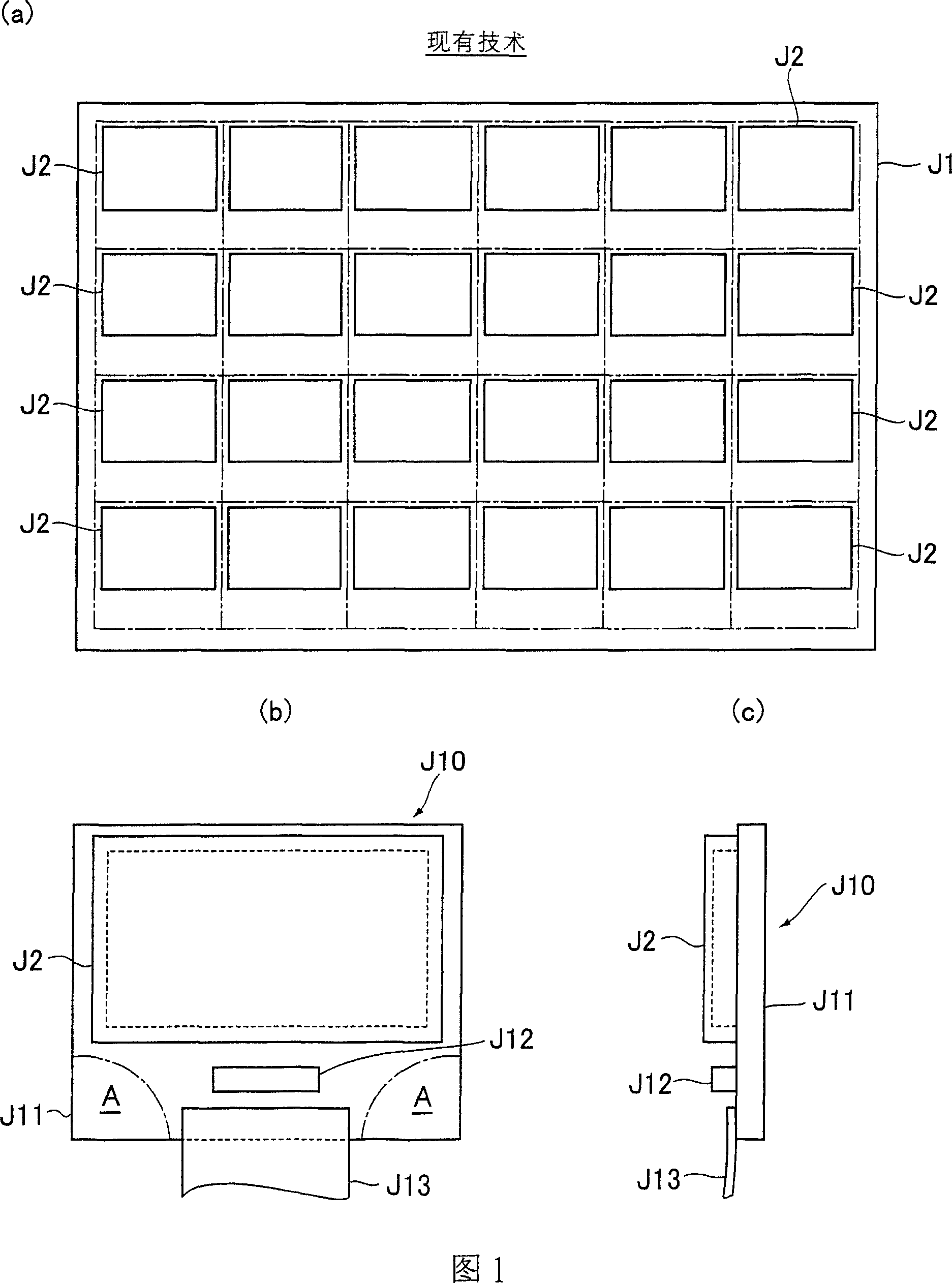
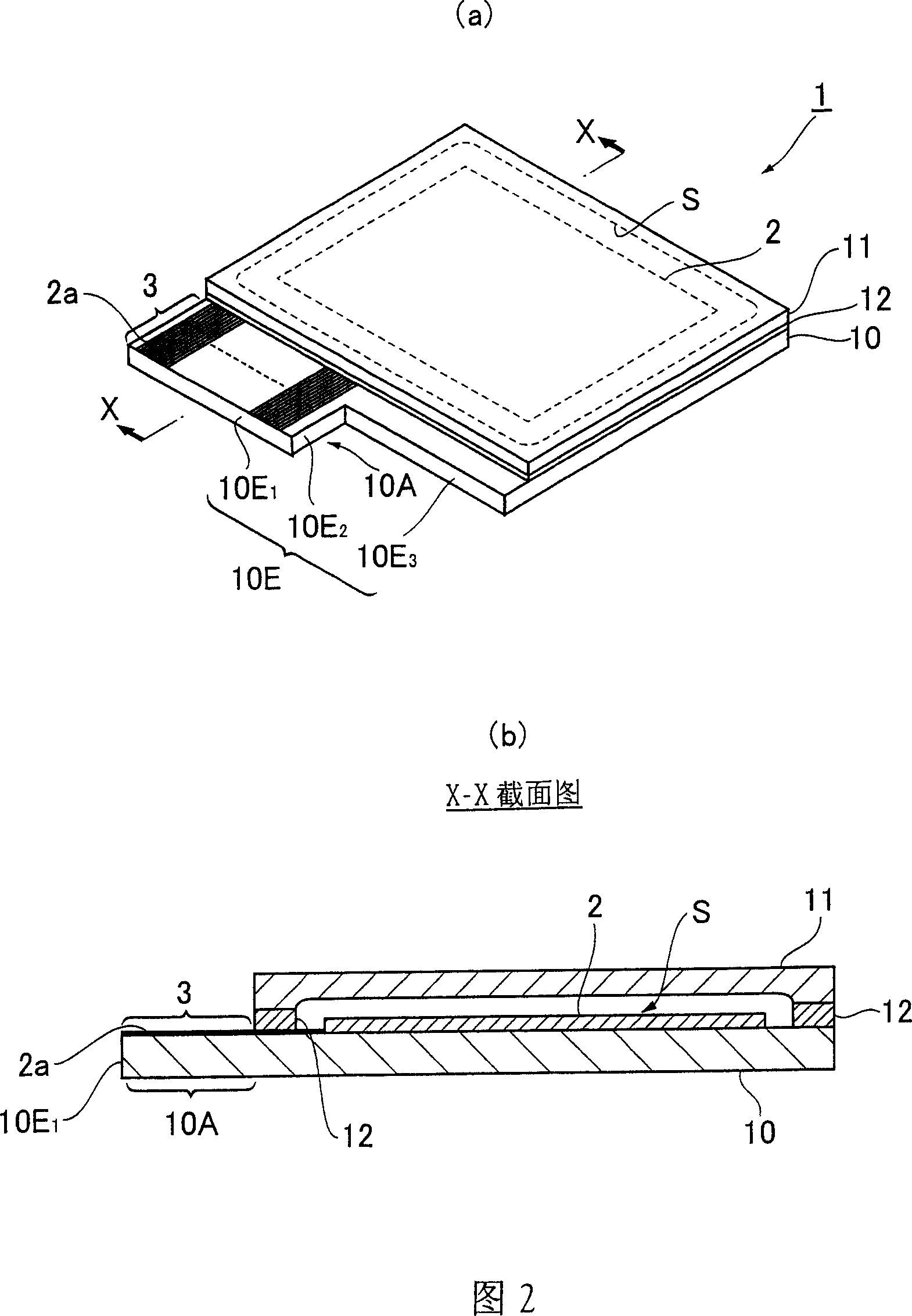
[0024] Hereinafter, embodiments of the present invention will be described with reference to the drawings. FIG. 2 is an explanatory view showing the overall structure of a self-luminous panel according to an embodiment of the present invention, in which FIG. 2( a ) shows an overall perspective view, and FIG. 2( b ) shows an X-X sectional view.

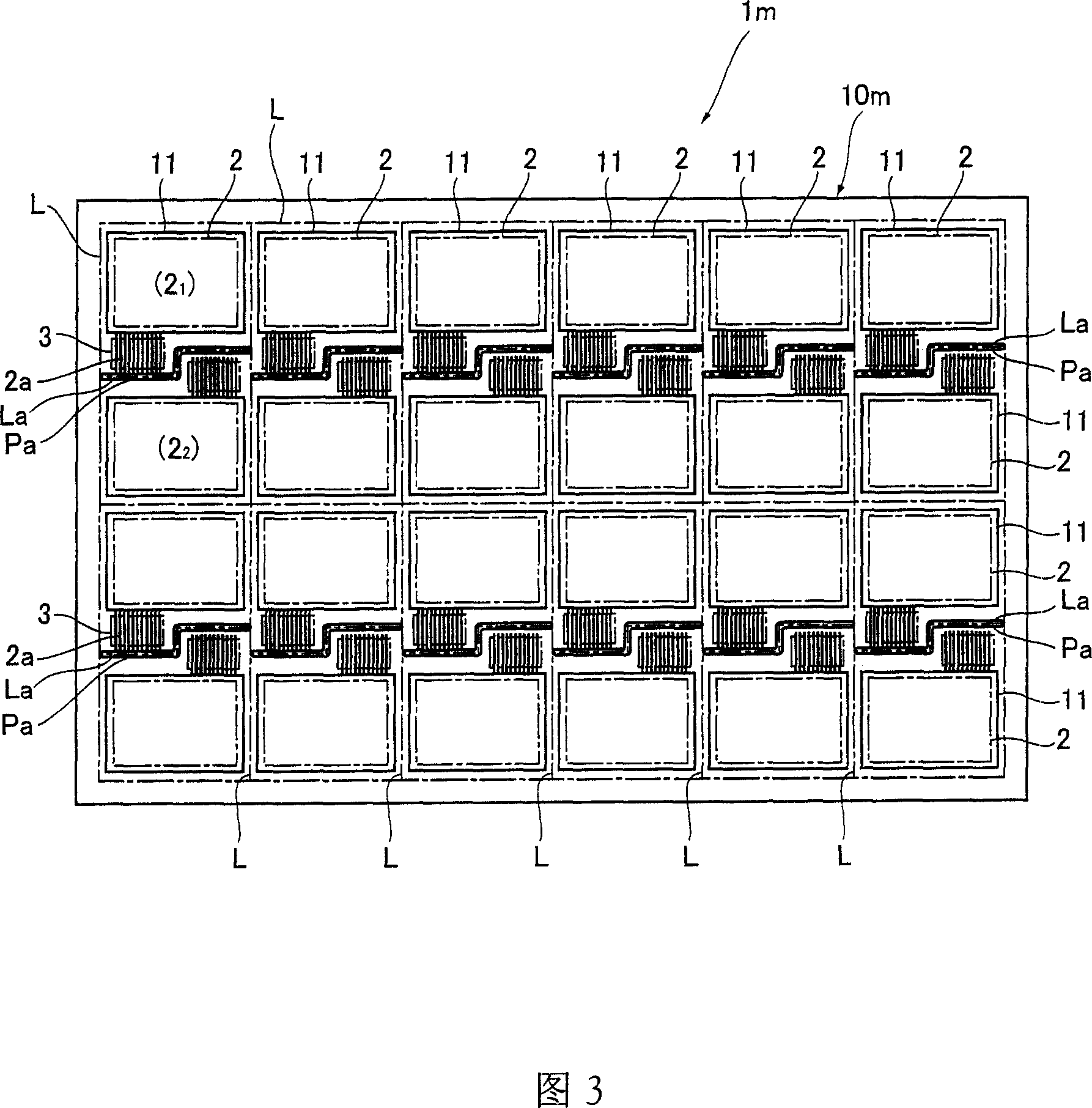
[0025] In the self-luminous panel 1, the self-luminous part 2 is formed on the support substrate 10, and the self-luminous part 2 is arranged in the sealing area S formed by bonding the support substrate 10 and the sealing member 11 through the adhesive layer 12, so that the self-luminous part 2 is formed. The connection part 3 of the lead wiring 2a drawn from the light-emitting part 2 to the outside of the sealing area S is formed on the support substrate 10 in an area other than the self-light-emitting part 2, and the connection part 3 connects the driver IC (not shown) and the flexible substrate. . In addition, an example in which ...


PUM


Abstract

The present invention relates to self-emission panel and a method of manufacturing the same to reduce an additional area in a self-emission panel substrate, ensure an acceptable number of divided substrates so as to reduce production cost. As a solvement means, the single self-emission panel is obtained by the following method: a plurality of sealed self-emission sections are formed on a mother support substrate, connecting sections formed with lead-out wiring portions led out from the self-emission sections are formed outside the self-emission sections on the mother support substrate; specifically, bent dividing lines for sectioning in parallel protrusion areas protruding from neighboring self-emission sections to form the connecting sections are set in areas between neighboring self-emission sections on the mother support substrate; further, hole processing portions are formed along partial or entire bent dividing lines, thereby making it possible to produce a plurality of unit self-emission panels simply by cutting along linear dividing lines.

Description

technical field [0001] The invention relates to a self-luminous panel and a manufacturing method thereof. Background technique [0002] Self-luminous panels represented by EL (Electroluminescent, electroluminescence) display panels, PDP (Plasma display panels, plasma display panels), FED (Field emission display, field emission display) panels, as flat panel displays and lighting components, etc., It is widely used in various electronic devices. In particular, organic EL panels, of course, can realize color display with desired luminance efficiency by using various colors of RGB, and also have the following characteristics. The driving voltage is as low as several to tens of volts, and can be obtained even when viewed from an oblique angle. High visibility, and relatively fast response to display switching, is also expected to achieve thinner or paper display (Paperdisplay). [0003] Such a self-luminous panel has a structure in which a self-luminous portion formed on a sup...

Claims


Application Information

Patent Timeline
Patent Type & Authority Applications(China)
IPC IPC(8): H01L51/50H01L51/52H01L51/56H05B33/12H05B33/02H05B33/10
CPCH01L51/56H01L51/5237H10K50/841H10K71/851H10K71/00
Inventor 会田俊春
Owner TOHOKU PIONEER CORP
Why Eureka
Try Eureka