


Quick Research
Generate reliable direction feasibility study reports for your R&D in just a few steps.

Technical Q&A
Discover and master advanced knowledge NOW. Basics, ideas, possibilities, all at once.

Find Solutions
As an expert in R&D theories, this can generate solutions to your technical problems instantly.

Evaluate Feasibility
Analyze your overall solution with one click, know your potential R&D risks in advance.

Monitor Landscape
Get weekly tech updates, stay abreast of the latest tech innovations and key insights.
Storage device and semiconductor device
一种存储设备、半导体的技术,应用在半导体器件、半导体/固态器件制造、静态存储器等方向,能够解决铁电薄膜技术困难、有延迟等问题
- Summary
- Abstract
- Description
- Claims
- Application Information
AI Technical Summary
Problems solved by technology
Method used
Image

Examples
Embodiment approach
[0049] Embodiments of the present invention will be described with reference to the accompanying drawings. However, the present invention is not limited to the following description, and it is easily understood by those skilled in the art that modes and details can be variously changed without departing from the scope and spirit of the present invention. Accordingly, the invention is not to be construed as being limited to the description of the various embodiments shown herein. It should be noted that reference numerals denoting like items may be used commonly in the drawings for structures described hereafter.
Embodiment approach 1
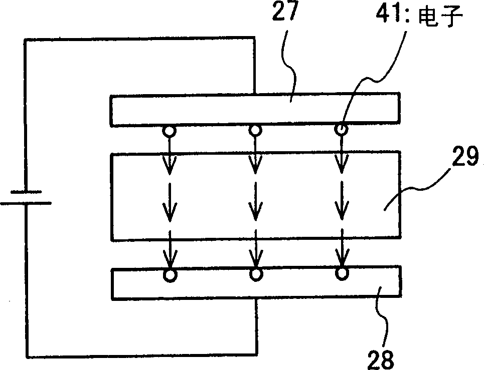
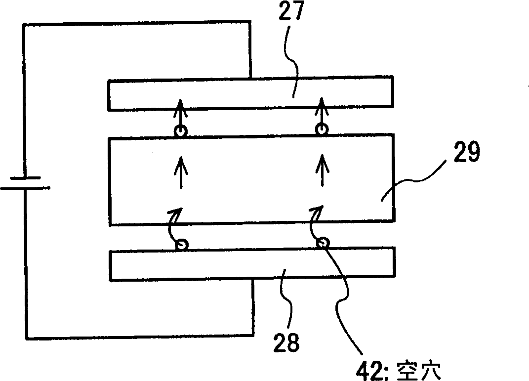
[0051] This embodiment mode will describe a structural example of a memory device (hereinafter also referred to as a memory circuit or an organic memory) in which an organic compound is provided between two conductive layers, see the drawings.
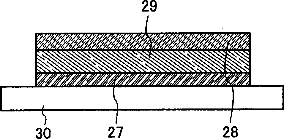
[0052] like figure 1 As shown, a glass substrate made of barium borosilicate glass, aluminoborosilicate glass, or the like, a quartz substrate, a ceramic substrate, or the like can be used as the substrate 30 . A metal substrate including stainless steel, or a semiconductor substrate on which an insulating layer is formed may also be used. Although substrates made of flexible synthetic resins of plastic such as PET generally tend to have a lower allowable temperature limit than the above substrates, it is still possible to use substrates made of flexible synthetic resins as long as the substrates can withstand the processing temperatures in the manufacturing steps. fabricated substrates.
[0053] As one or both of the first conductiv...
Embodiment approach 2
[0075] This embodiment mode will describe a structural example of a memory circuit including an organic compound layer in a memory element portion with reference to the drawings. More specifically, this embodiment mode will show the case of a memory circuit having a passive matrix structure.
[0076] Figure 5A A structural example of a semiconductor device of the present invention is shown, including: a memory cell array 22 in which memory cells 21 are arranged in a matrix form; a bit line driver circuit 26 having a column decoder 26a, a read circuit 26b, and a selector 26c; A line driver circuit 24 having a row decoder 24a and a level shifter 24b; and an interface 23 having a writing circuit and the like to communicate with the outside. Note that the structure of the memory circuit 16 shown here is only an example, and the memory circuit 16 may also include other circuits such as a sense amplifier, an output circuit, and a buffer circuit, and in addition, a write circuit ma...
PUM
 Abstract
Description
Claims
Application Information
 - R&D Engineer
- R&D Manager
- IP Professional
- Industry Leading Data Capabilities
- Powerful AI technology
- Patent DNA Extraction
Browse by: Latest US Patents, China's latest patents, Technical Efficacy Thesaurus, Application Domain, Technology Topic, Popular Technical Reports.
© 2024 PatSnap. All rights reserved.Legal|Privacy policy|Modern Slavery Act Transparency Statement|Sitemap|About US| Contact US: help@patsnap.com