


Quick Research
Generate reliable direction feasibility study reports for your R&D in just a few steps.

Technical Q&A
Discover and master advanced knowledge NOW. Basics, ideas, possibilities, all at once.

Find Solutions
As an expert in R&D theories, this can generate solutions to your technical problems instantly.

Evaluate Feasibility
Analyze your overall solution with one click, know your potential R&D risks in advance.

Monitor Landscape
Get weekly tech updates, stay abreast of the latest tech innovations and key insights.
Memory
A memory and memory cell technology, applied in the field of memory, can solve problems such as the increase in the size of memory cells
- Summary
- Abstract
- Description
- Claims
- Application Information
AI Technical Summary
Problems solved by technology
Method used
Image

Examples
no. 1 approach
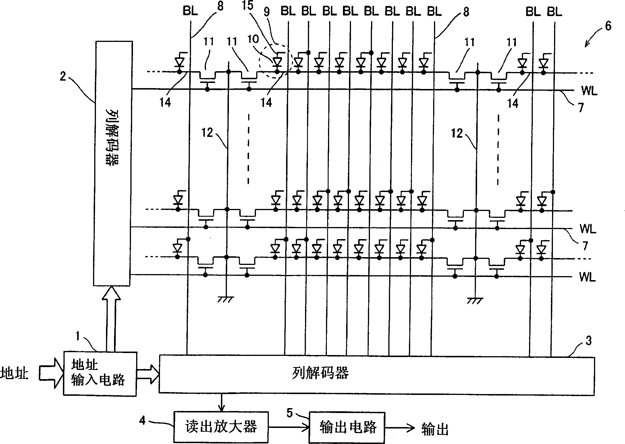
[0047] refer to Figure 1 ~ Figure 4 , the configuration of the mask ROM according to the first embodiment of the present invention will be described.
[0048] Such as figure 1 As shown, the mask ROM of the first embodiment includes an address input circuit 1 , a row decoder 2 , a column decoder 3 , a sense amplifier 4 , an output circuit 5 , and a memory cell array 6 . In addition, a peripheral circuit is constituted by an address input circuit 1 , a row decoder 2 , a column decoder 3 , a sense amplifier 4 and an output circuit 5 . Address input circuit 1 outputs address data to row decoder 2 and column decoder 3 by inputting a predetermined address from the outside. In addition, a plurality of word lines (WL) 7 are connected to the column decoder 2 . Row decoder 2 receives address data from address input circuit 1, selects word line 7 corresponding to the input address data, and raises the potential of selected word line 7 to H level. In addition, a plurality of bit lin...
no. 2 approach
[0099] refer to Figure 23 ~ Figure 28 , the configuration of the MRAM (Magnetic Random Access Memory) according to the second embodiment of the present invention will be described. In this second embodiment, a cross-point type MRAM will be described by taking an example in which the drain region of the select transistor and the cathode of the diode included in the memory cell are formed by a common impurity region.
[0100] In the MRAM of the second embodiment, as Figure 23 As shown, each memory cell 59 arranged in the memory cell array 56 includes a diode 60 and a TMR (Tunneling Magneto Resistance) element 62 . In addition, one electrode of the TMR element 62 is connected to the anode of the diode 50 , and the other electrode is connected to the bit line (BL) 8 . The circuit configuration of the MRAM of the second embodiment other than the above is the same as the circuit configuration of the mask ROM of the first embodiment.
[0101] Additionally, the TMR element 62 as ...
no. 3 approach
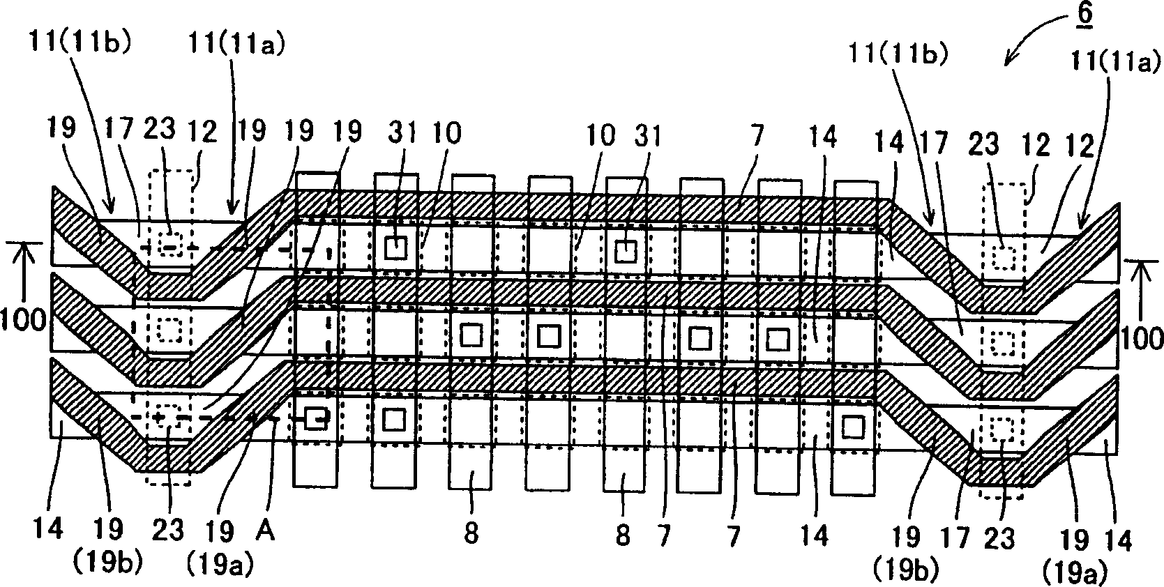
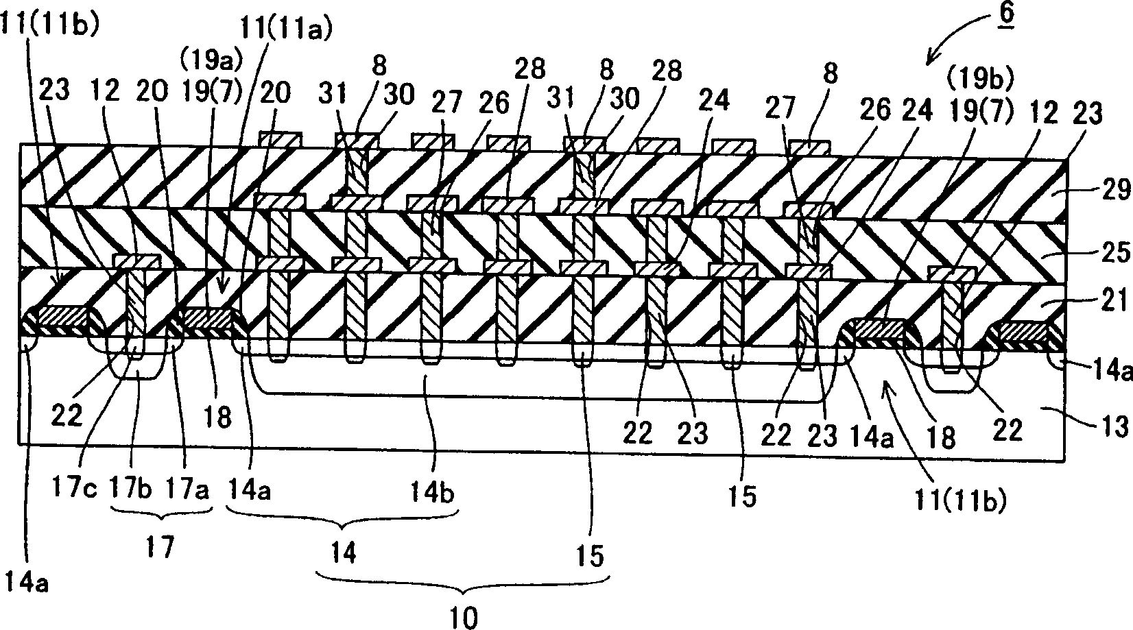
[0116] Figure 32 It is a plan layout diagram showing the structure of the mask ROM according to the third embodiment of the present invention. Figure 33 is zoomed in Figure 32 An enlarged plan view of a dotted-line region D of the mask ROM according to the third embodiment of the present invention is shown. Next, refer to Figure 32 and Figure 33 , the structure of the mask ROM according to the third embodiment of the present invention will be described.
[0117] In the third embodiment mask ROM, such as Figure 32 and Figure 33 As shown, unlike the mask ROM of the above-mentioned first embodiment, the n-type impurity region 114 and the source region 117 serving as the drain region on the formation region of the selection transistor 11a and the gate electrode 19a are extended in an oblique direction. The vicinity of the intersecting part, so that the top view, with the figure 1 The extending direction of the n-type impurity region 114 on the formation region of th...
PUM
 Abstract
Description
Claims
Application Information
 - R&D Engineer
- R&D Manager
- IP Professional
- Industry Leading Data Capabilities
- Powerful AI technology
- Patent DNA Extraction
Browse by: Latest US Patents, China's latest patents, Technical Efficacy Thesaurus, Application Domain, Technology Topic, Popular Technical Reports.
© 2024 PatSnap. All rights reserved.Legal|Privacy policy|Modern Slavery Act Transparency Statement|Sitemap|About US| Contact US: help@patsnap.com