


Quick Research
Generate reliable direction feasibility study reports for your R&D in just a few steps.

Technical Q&A
Discover and master advanced knowledge NOW. Basics, ideas, possibilities, all at once.

Find Solutions
As an expert in R&D theories, this can generate solutions to your technical problems instantly.

Evaluate Feasibility
Analyze your overall solution with one click, know your potential R&D risks in advance.

Monitor Landscape
Get weekly tech updates, stay abreast of the latest tech innovations and key insights.
Display device
A technology for a display device and a display panel, which is applied in the fields of display devices with voltage drop and scanning circuits, can solve the problems of large parasitic capacitance of column wiring, increased power consumption of data driver, and increased voltage amplitude of column wiring, etc., so as to reduce the amplitude of output voltage. , reduce power consumption, and correct the effect of small errors
- Summary
- Abstract
- Description
- Claims
- Application Information
AI Technical Summary
Problems solved by technology
Method used
Image


Examples
Embodiment 1
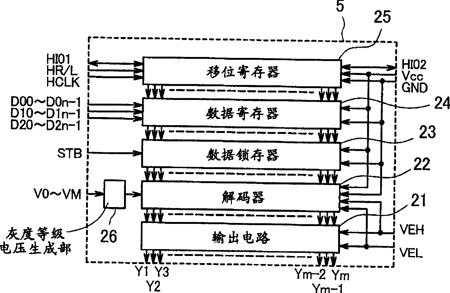
[0054] figure 1 is a block diagram showing the overall circuit configuration (1) of this embodiment. The display panel 4 includes a back panel, a front panel and side walls (not shown). The backplane has column wiring 1 extending vertically (Y direction), row wiring 2 extending laterally (X direction), and electron emission elements 3 connected to one column wiring and one row wiring. A plurality of column wirings are arranged horizontally, and a plurality of row wirings are arranged vertically. The electron emission element is a MIM type electron emission element. The front plate has a fluorescent film 10 and a back gold 11 formed to cover the fluorescent film 10 . The surface of the back plate on which the electron emission elements 3 are formed is opposed to the surface of the front plate on which the fluorescent surface is formed, and the side walls are arranged on the opposing surfaces of the front plate and the back plate. The panel is internally vented.
[0055] F...
Embodiment 2
[0122] In Embodiment 1 described above, there are cases where an overshoot occurs when the output voltage Gn of the output circuit rises from the non-selection voltage VGL to the selection voltage VGH, making it difficult to control the amount of light emission with high precision.
[0123] The delay caused by the on-resistance of the pMOS selection switch 41 and the wiring capacitance of the row wiring 2, and the delay caused by the wiring capacitance of the pMOS detection switch 43 and the input wiring 46 of the differential amplifier 44 make the input voltage of the differential amplifier 44 change slowly. changes in the output voltage, thereby causing this overshoot.
[0124] In this embodiment, the turning-off timing of the pMOS feedback switch 45 is set later than the turning-on timing of the pMOS selection switch 41 and the pMOS detection switch 43 of the selected row.
[0125] Figure 8 Indicates the output timing of the data driver and the scan driver within one hori...
Embodiment 3
[0131] In this embodiment, the data driver output voltage is corrected in consideration of the resistance Ro2 from the output point of the scan driver to the pixels at both ends in the second embodiment. Figure 9 It is a diagram explaining the row wiring voltage drop and the state of correction at this time.
[0132] exist Figure 9 , mark 3, r, Ro, im and Figure 6 Same, mark iRm', iLm', Vm', Im', VVL', VVR' and Figure 6 iRm, iLm, Vm, Im, VVL, VVR are the same. In addition, Ro2 is the resistance from the output point of the scan driver to the pixels at both ends.
[0133] The row wiring voltage drop Vm' generated in the mth pixel is obtained as follows. The correction values VVL' and VVR' are respectively input to the output circuit of the scan driver, so that the voltage drop at the output point of the scan driver becomes zero, and the output point of the scan driver becomes a virtual point.
[0134] The diode current im of the m-th pixel consists of two components ...
PUM
 Abstract
Description
Claims
Application Information
 - R&D Engineer
- R&D Manager
- IP Professional
- Industry Leading Data Capabilities
- Powerful AI technology
- Patent DNA Extraction
Browse by: Latest US Patents, China's latest patents, Technical Efficacy Thesaurus, Application Domain, Technology Topic, Popular Technical Reports.
© 2024 PatSnap. All rights reserved.Legal|Privacy policy|Modern Slavery Act Transparency Statement|Sitemap|About US| Contact US: help@patsnap.com