Chip flame storage box

A technology for storing boxes and wafers, which is applied in the manufacture of electrical components, semiconductor/solid-state devices, circuits, etc., and can solve the problems of increasing manufacturing costs, affecting the quality of wafers 12, wasting wafers 12, etc.

Inactive Publication Date: 2006-06-14
POWER GEODE TECH
View PDF0 Cites 3 Cited by
  • Summary
  • Abstract
  • Description
  • Claims
  • Application Information

AI Technical Summary

Problems solved by technology

If the wafer is stored in the wafer storage box 11, static electricity will be generated due to the friction between the surface of the wafer 12 and the sponge pad 13, which will affect the quality of the wafer 12.
In addition, in the process of handling, it is easy to increase the fragmentation rate of the wafer 12 due to improper impact, and a lot of wafers 12 are wasted virtually, thus increasing the manufacturing cost

Method used


Image

  • Chip flame storage box
  • Chip flame storage box
  • Chip flame storage box

Examples


Embodiment Construction

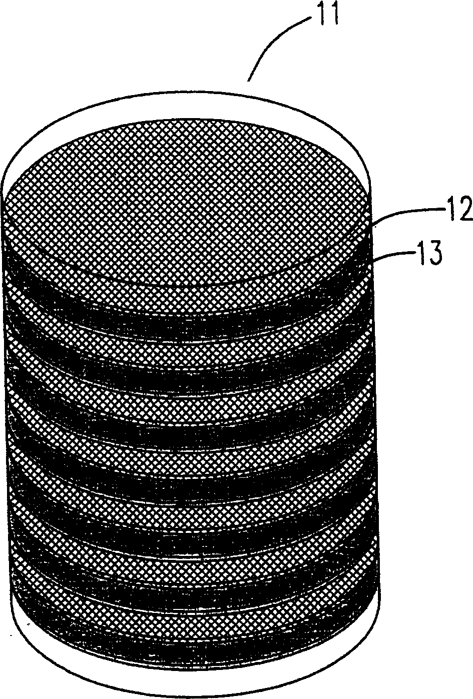
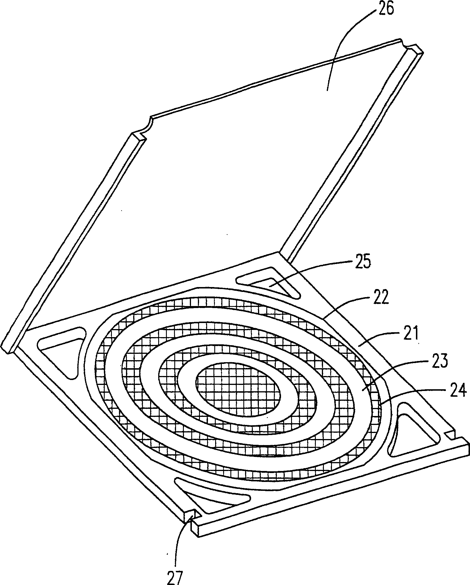
[0035] Please refer to FIG. 2( a ), which is a structural diagram of a Frame Storage Box (FSB) according to a preferred embodiment of the present invention. The wafer frame storage box includes a body 21 and a cover 26 , wherein the cover 26 is combined with the body 21 . The main body 21 has an accommodating space 22 , and a plurality of ring-shaped ribs 23 are formed on the bottom surface of the accommodating space 22 for strengthening the strength of the main body 21 . In addition, a plurality of anti-vibration pads 24 are arranged on the bottom surface of the accommodating space 22, and the anti-vibration pads 24 can reduce the external impact force received by the wafer during the process of transferring the wafer, thus effectively reducing the fragmentation rate of the wafer. To save manufacturing cost.

[0036] Four perforations 25 are provided at four corners of the main body 21 to facilitate the user to pick up the wafer frame storage box with fingers and reduce the ...


PUM


Abstract

The invention relates to a wafer frame storage box, for storing a wafer, comprising: a main body with a holding space; plural saliencies formed on the bottom surface of the holding space to reinforce the main body; plural shockproof components arranged in the bottom surface of the holding space; and a cover body integrated with the main body. In the course of carrying wafers, it can reduce the received external shock force and thus effectively reduce the wafer chipping ratio so as to save the manufacturing cost.

Description

technical field [0001] The invention relates to a wafer frame storage box, in particular to a wafer frame storage box which can reduce the wafer fragmentation rate. Background technique [0002] In the manufacture of semiconductors, many different processes are included. During the conversion between processes, it is inevitable to store and transport wafers. At this time, wafer storage boxes must be used to store wafers. [0003] see figure 1 , which is a schematic structural view of a known wafer storage box. The wafer storage box 11 is a plastic box for storing a plurality of wafers 12. The number of wafers 12 stored depends on the capacity of the wafer storage box 11. Only a sponge pad 13 is used as a gap between each wafer 12. If the wafer is stored in the wafer storage box 11 , static electricity will be generated due to the friction between the surface of the wafer 12 and the sponge pad 13 , thereby affecting the quality of the wafer 12 . In addition, in the process...

Claims


Application Information

Patent Timeline
IPC IPC(8): H01L21/68
Inventor 刘育钏
Owner POWER GEODE TECH
Why Eureka
Try Eureka