Semiconductor device
A semiconductor and conductive technology, applied in the direction of semiconductor devices, transistors, electric solid devices, etc., can solve the problems of limited low on-resistance, influence on the substrate, long current path, etc., to suppress the increase of resistance and reduce the conduction Effect of resistance, amount of reduction
- Summary
- Abstract
- Description
- Claims
- Application Information
AI Technical Summary
Problems solved by technology
Method used
Image

Examples
Embodiment Construction
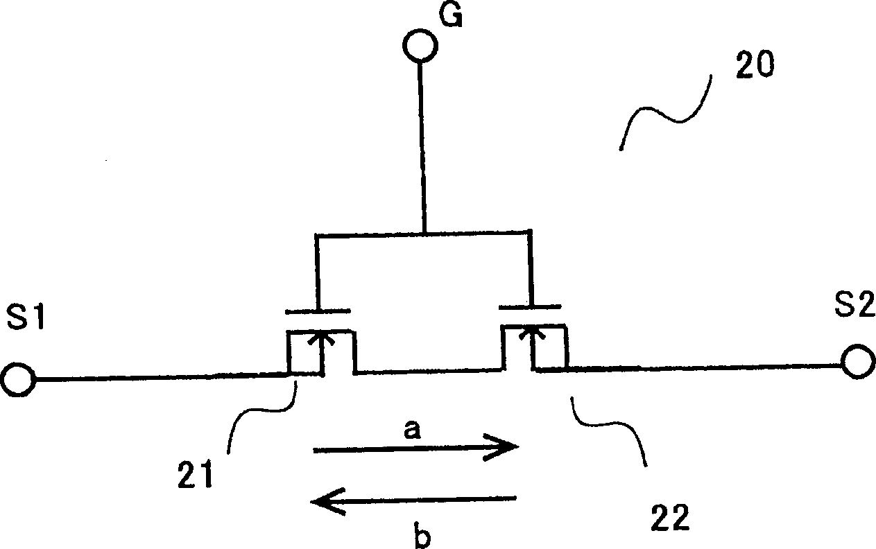
[0076] Take n-channel MOSFET as an example for reference Figure 1 to Figure 4 Embodiments of the present invention will be described in detail.
[0077] figure 1 It is a circuit schematic diagram showing the semiconductor device 20 of this embodiment.
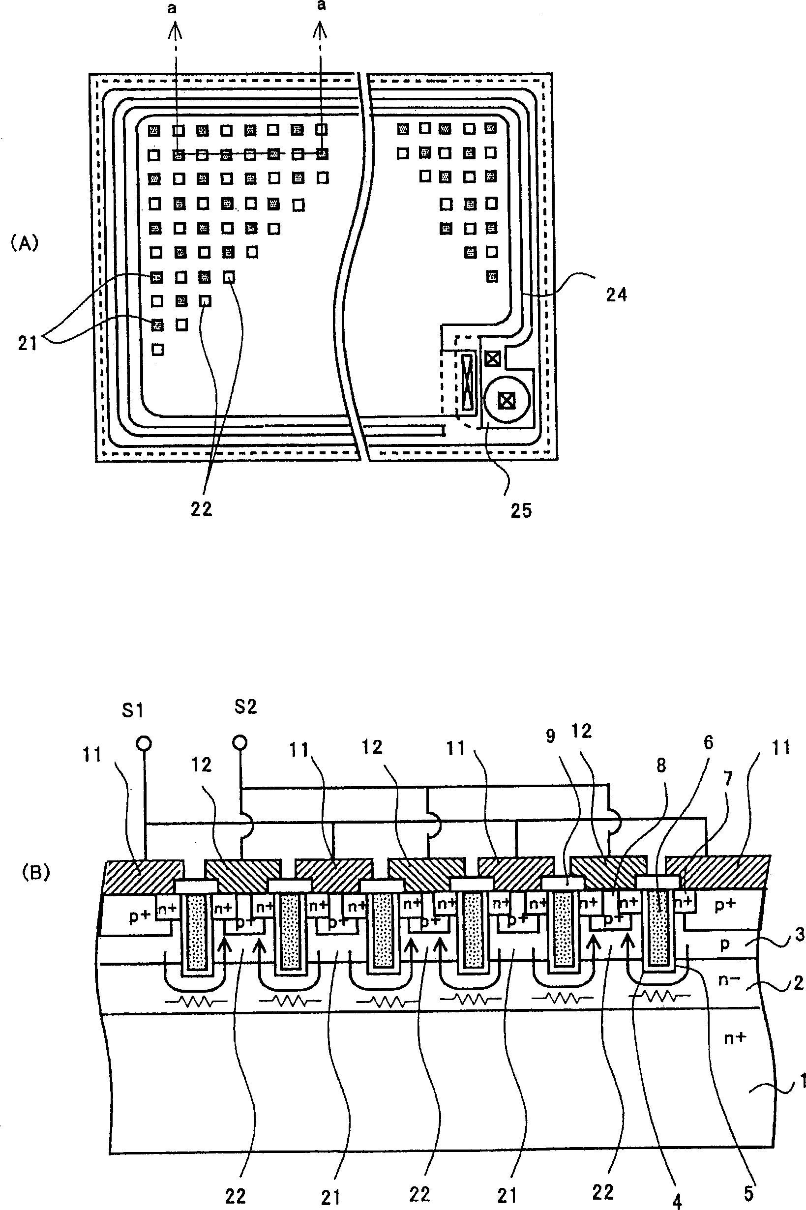
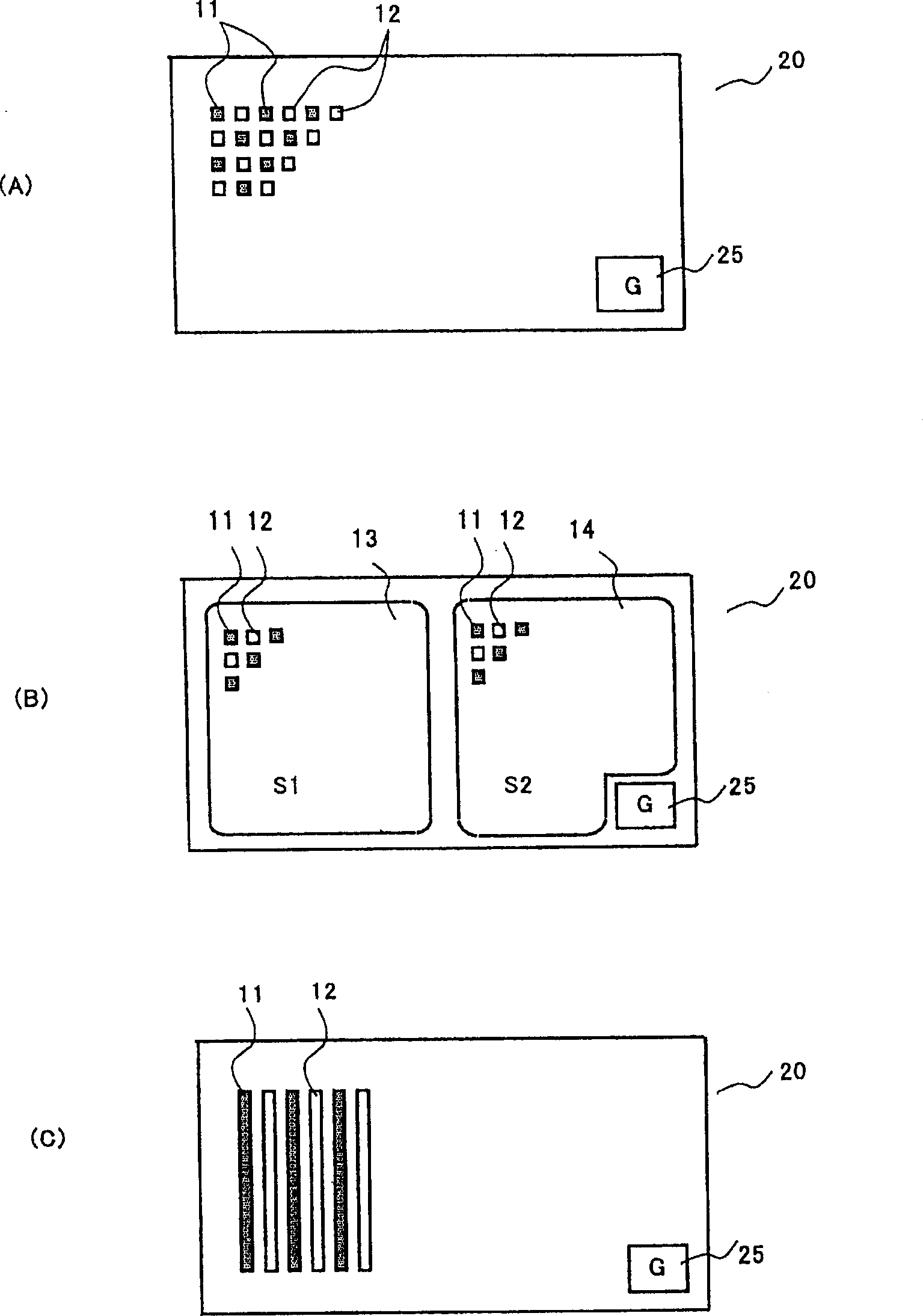
[0078] The semiconductor device 20 of this embodiment is a MOSFET in which a plurality of MOS transistors 21 and 22 are arranged on a semiconductor substrate constituting a drain region. The MOSFET 20 is connected to a gate terminal G and is controlled by a control signal applied to the gate terminal G.
[0079] The MOS transistors 21 and 22 are integrated on one chip, and the terminals leading out to the outside are a gate terminal, a first source terminal S1, and a second source terminal S2. In addition, the drains of the plurality of MOS transistors 21 and 22 are connected in common, and are not led out to the outside as drain terminals.
[0080] Different potentials are applied to the first source terminal S1 and the ...
PUM
 Abstract
Description
Claims
Application Information
 - Generate Ideas
- Intellectual Property
- Life Sciences
- Materials
- Tech Scout
- Unparalleled Data Quality
- Higher Quality Content
- 60% Fewer Hallucinations
Browse by: Latest US Patents, China's latest patents, Technical Efficacy Thesaurus, Application Domain, Technology Topic, Popular Technical Reports.
© 2025 PatSnap. All rights reserved.Legal|Privacy policy|Modern Slavery Act Transparency Statement|Sitemap|About US| Contact US: help@patsnap.com