Solid-state image pickup device and camera using the same solid-state image pickup device
一种摄像装置、固态的技术,应用在辐射控制装置、图像通信、彩色电视的零部件等方向
- Summary
- Abstract
- Description
- Claims
- Application Information
AI Technical Summary
Problems solved by technology
Method used
Image
Examples
no. 1 approach
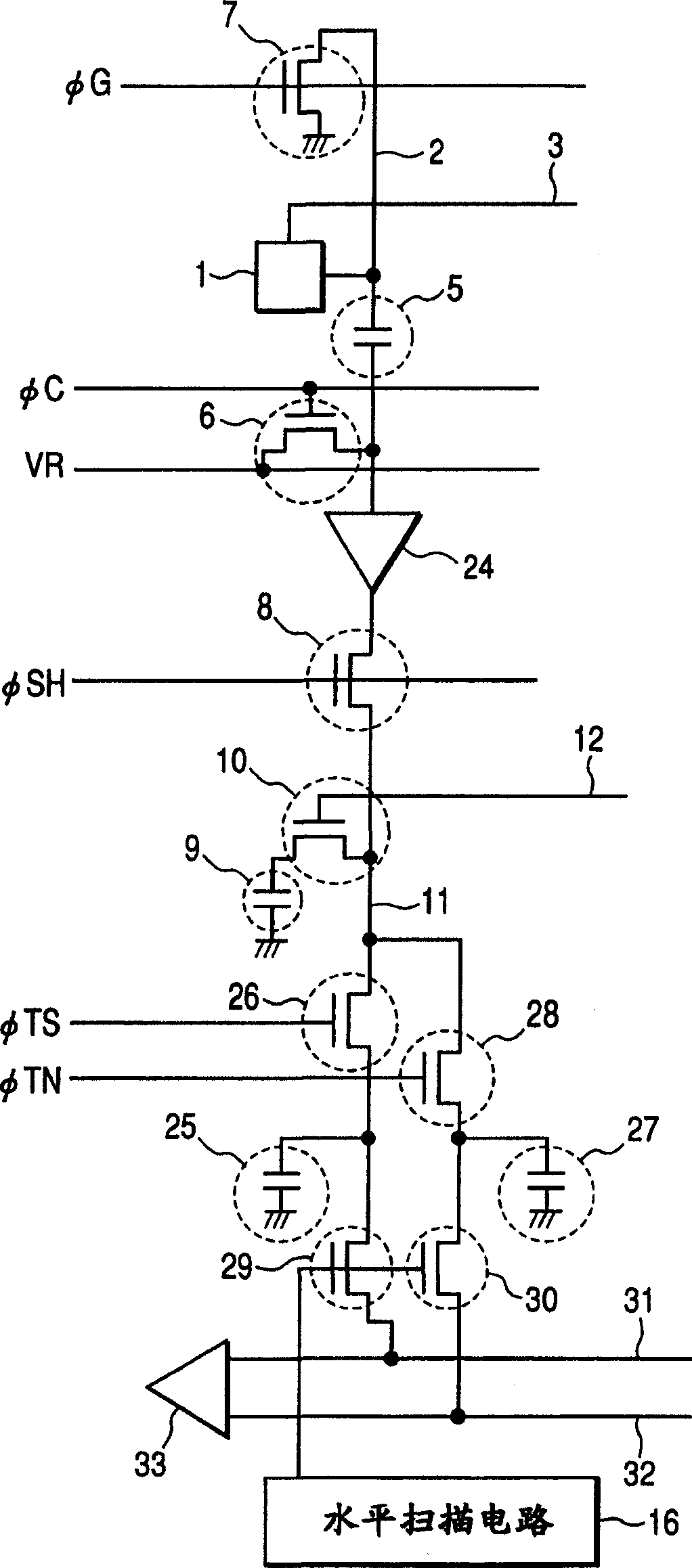
[0031] figure 1 A circuit diagram of a sensor along a signal path from a pixel to a sensor output in the first embodiment of the present invention is shown. Here, for the sake of simplicity, it is represented by one pixel, one storage unit, and one column of readout devices. In fact, it is as follows Figure 8 As shown, the pixels and memory cells are arranged in a two-dimensional shape, and the readout devices are arranged in columns. and in Figure 8 For simplicity, the pixels and storage units are represented by 3×3 pixels and storage units respectively, but the number of pixels and the number of storage units can also be set as required, and the number of storage units can be less than the number of pixels. For example, when signals from multiple pixels are summed or stored in memory cells at long intervals, the number of memory cells can be smaller than the number of pixels, but in order to form an image, the number of memory cells corresponding to the number of necessar...
no. 2 approach
[0039] image 3 A sensor circuit diagram showing a signal path from a pixel to a sensor output in the second embodiment of the present invention. exist image 3 Among them, the column amplifier 24 is a feedback type amplifier, and its output is transmitted to the negative input terminal through the coupling capacitor 34 . Therefore, the gain of the column amplifier 24 is determined by the ratio between the coupling capacitor 5 and the coupling capacitor 34 . The positive input terminal (+) is fixed at the clamp potential VR. The negative input terminal (−) is clamped to the clamp potential VR by applying the pulse [phi]C to the clamp transistor 6 . This is because the above-mentioned two input terminals are in a virtual short-circuit state. As a result, the pulse time for the action of this sensor structure is the same as figure 2 The pulse times for the first embodiment shown are the same. but, image 3 The circuit in has the feature that the coupling capacitor 5 used...
no. 3 approach
[0041] Figure 4 A sensor circuit diagram showing a signal path from a pixel to a sensor output in a third embodiment of the present invention. In this figure, the memory with the amplification function in the cell is used. For example, a structure disclosed in US Pat. No. 5,805,492, an amplified analog memory cell is known. exist Figure 4 Among them, the memory cell 35 is composed of an amplification transistor 36 , a memory selection transistor 37 , a write transistor 10 and a memory cell capacitor 9 .
[0042] The current feeding transistor 38 supplies a current to operate the amplifier transistor 36 as a source follower. In the third embodiment of the present invention, this amplified frame memory is used instead of the DRAM type memory used in the first and second embodiments.
[0043] Figure 5 is a pulse time chart showing the operation of the sensor according to the third embodiment of the present invention. according to Figure 4 , Figure 5 Description of th...
PUM
 Abstract
Description
Claims
Application Information
 - R&D
- Intellectual Property
- Life Sciences
- Materials
- Tech Scout
- Unparalleled Data Quality
- Higher Quality Content
- 60% Fewer Hallucinations
Browse by: Latest US Patents, China's latest patents, Technical Efficacy Thesaurus, Application Domain, Technology Topic, Popular Technical Reports.
© 2025 PatSnap. All rights reserved.Legal|Privacy policy|Modern Slavery Act Transparency Statement|Sitemap|About US| Contact US: help@patsnap.com


