Semiconductor device and method for fabricating the same

一种制造方法、半导体的技术,应用在半导体/固态器件制造、半导体器件、电气元件等方向,能够解决控制范围缩小等问题,达到提高穿通耐压、扩大控制范围的效果

Inactive Publication Date: 2005-08-24
コラボイノベーションズインコーポレイテッド
View PDF1 Cites 9 Cited by
  • Summary
  • Abstract
  • Description
  • Claims
  • Application Information

AI Technical Summary

Problems solved by technology

As a result, in a semiconductor device having a conventional trench gate structure, there is a problem that the control range of the valve voltage Vt is narrowed if the punch-through withstand voltage is lowered.

Method used


Image

  • Semiconductor device and method for fabricating the same
  • Semiconductor device and method for fabricating the same
  • Semiconductor device and method for fabricating the same

Examples


Embodiment approach 1

[0030] —Manufacturing of semiconductor devices—

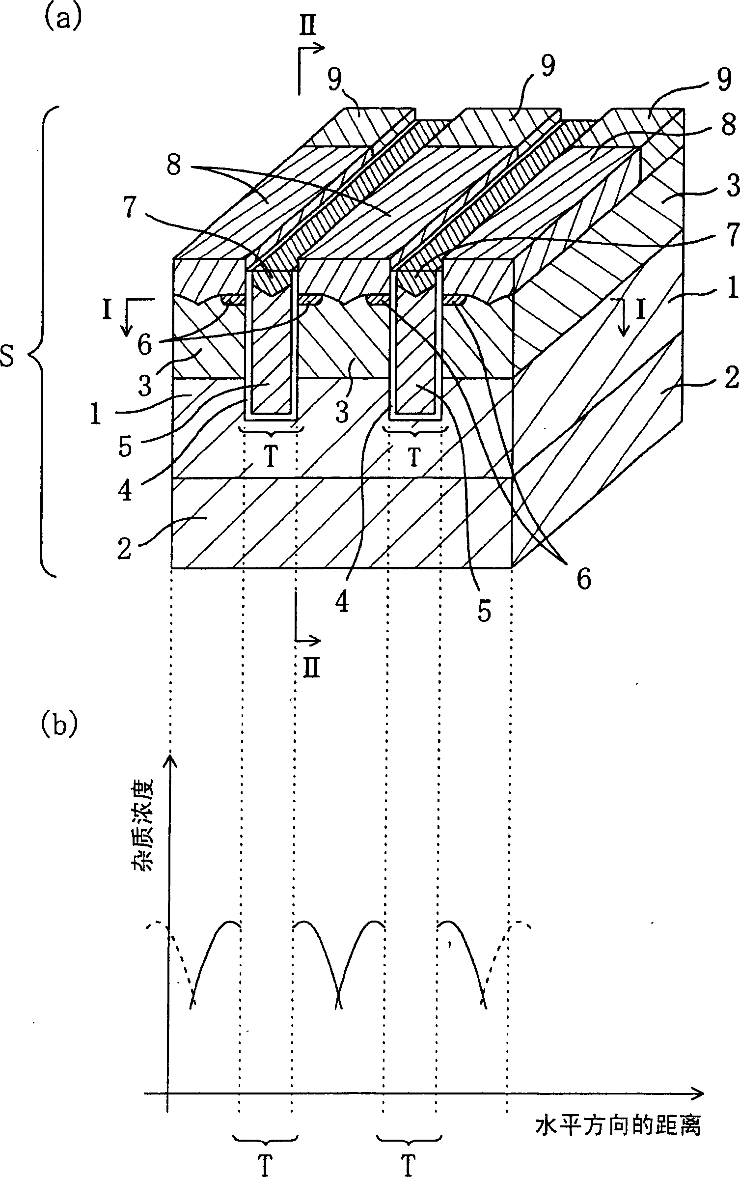
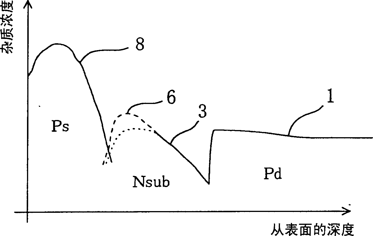
[0031] figure 1 (a) and (b) are perspective views showing the structure of the semiconductor device having the trench gate structure in Embodiment 1, and diagrams showing impurity concentration distribution along a cross-section shown by line I-I. In addition, in figure 1 In (a), the pairs of Figure 4 (c) A representation of the silicide layer 10 shown.

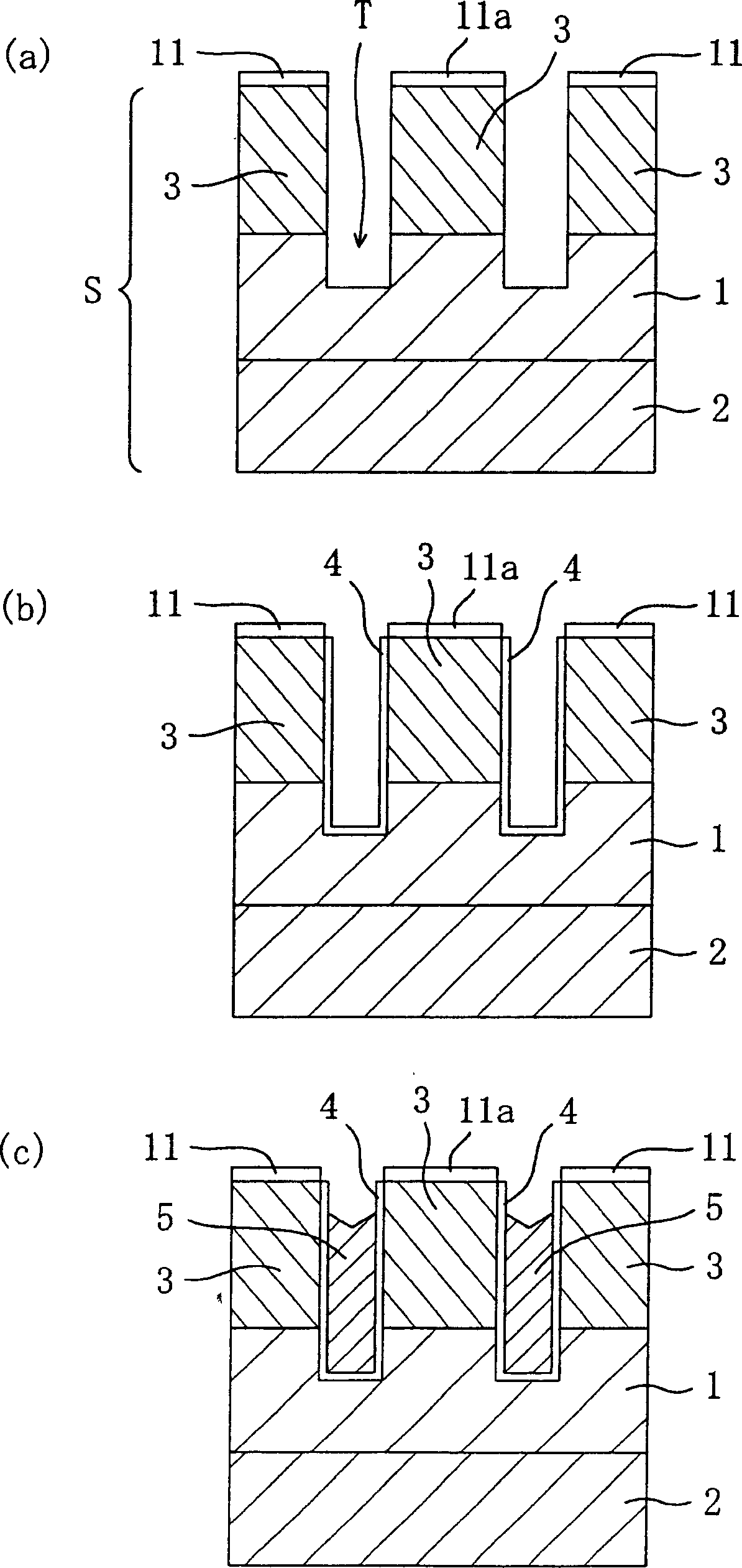
[0032] Such as figure 1 As shown in (a), the semiconductor device of this embodiment includes: a high-concentration P-type drain region 2 formed on a silicon substrate S, and a low-concentration P-type drain region (EPI) 1 provided on the high-concentration P-type drain region 2 , a high-concentration P-type source region 8 formed above the low-concentration drain region 1 , and an N-type substrate region 3 formed between the high-concentration P-type source region 8 and the low-concentration P-type drain region (EPI) 1 . In addition, a trench T for forming a gate ele...

Embodiment approach 2

[0052] —Structure of semiconductor device—

[0053] Figure 6 (a) and (b) are perspective views showing the structure of a semiconductor device having a trench gate structure according to Embodiment 2 of the present invention, and diagrams showing impurity concentration distribution along a cross section indicated by line VI-VI. In addition, in Figure 6 In (a), for the sake of easy to see the structure, the pair Figure 5 (c) A representation of the silicide layer 10 shown. The structure of the semiconductor device of this embodiment is basically the same as that of Embodiment 1 (see figure 1 (a)) are the same, and therefore descriptions of parts having the same structure are omitted.

[0054] Such as Figure 6 As shown in (a), in the semiconductor device of this embodiment, the N-type pocket region 6B is formed in the entire region between the N-type substrate region 3 and the high-concentration P-type source region 8 . That is, in the semiconductor device of the pres...


PUM


Abstract

Provided is a semiconductor device with a trench gate structure having a high punch-through withstand voltage and a wide control range for the threshold voltage Vt, and to provide its manufacturing method. A semiconductor device is provided with a p-type drain region that is formed into a silicon substrate S; a low-concentration p-type drain region (EPI)1; a high-concentration p-type source region 8 that is formed at the upper part of the low-concentration drain region 1; an n-type substrate region 3 that is formed between the high-concentration p-type source region 8 and the low-concentration p-type drain region (EPI)1, a trench T; a gate insulating film 4 and a gate electrode 5 that are formed inside the trench T, an insulating film 7 closing the trench T; and an n-type pocket region 6 that is formed between the n-type substrate region 3 and the high-concentration p-type source region 8. By the n-type pocket region 6, there is formed a barrier blocking the spread of a depletion layer from the low-concentration p-type drain region 1, without reinforcing the electric field strength applied to the low-concentration p-type drain region 1 side.

Description

technical field [0001] The present invention relates to a semiconductor device with a trench MIS (Metal-Insulator-Semiconductor) gate structure and a manufacturing method thereof. Background technique [0002] For a long time, a trench gate structure formed by forming a trench in a semiconductor substrate and burying a gate electrode in the trench has been applied to semiconductors such as IGBT (Insulated Gate Bipolar Transistor) or MISFET (Field Effect Transistor). This structure is very useful in applications such as electric power in particular. For example, IGBTs with a trench gate structure have both the high input impedance characteristics of MISFETs and the low saturation voltage characteristics of bipolar transistors, and are widely used in uninterruptible power supply devices and various motor drive devices. [0003] Figure 8 A perspective view showing a semiconductor device having a conventional trench MOS gate structure disclosed in Patent Document 1. FIG. As s...

Claims


Application Information

Patent Timeline
Patent Type & Authority Applications(China)
IPC IPC(8): H01L29/78H01L21/265H01L21/331H01L21/336H01L29/10H01L29/43H01L29/45H01L29/739
CPCH01L29/66734H01L29/7813H01L29/456H01L21/26586H01L29/7397H01L29/66348H01L29/1095
Inventor 宫口里江沟口修二
Owner コラボイノベーションズインコーポレイテッド
Why Eureka
Try Eureka