Light emitting diode
A technology of light-emitting diodes and light injection, which is applied in optics, light guides, optical components, etc., and can solve problems such as the inability to install ultra-thin mobile phones
- Summary
- Abstract
- Description
- Claims
- Application Information
AI Technical Summary
Problems solved by technology
Method used
Image
Examples
Embodiment approach 1
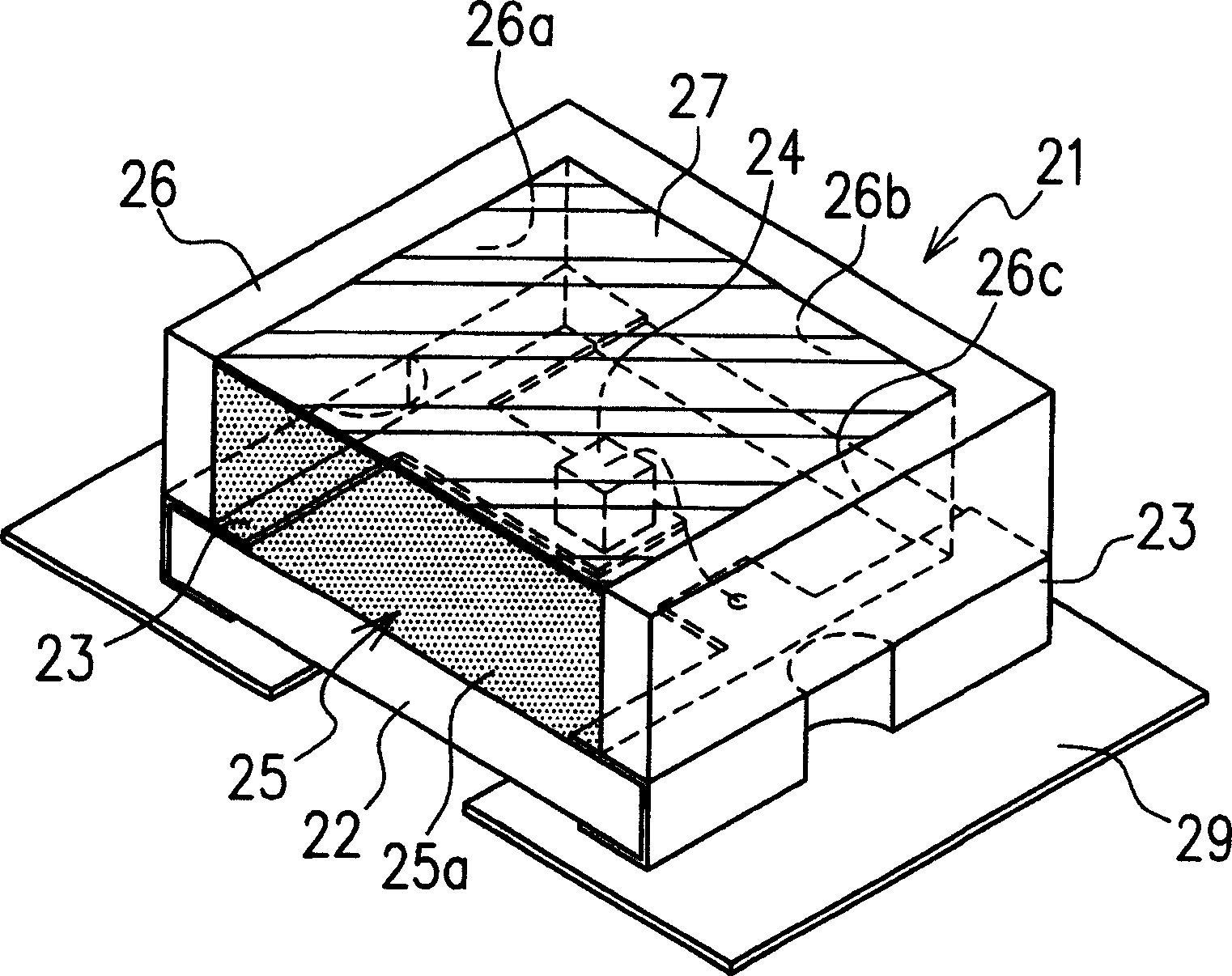
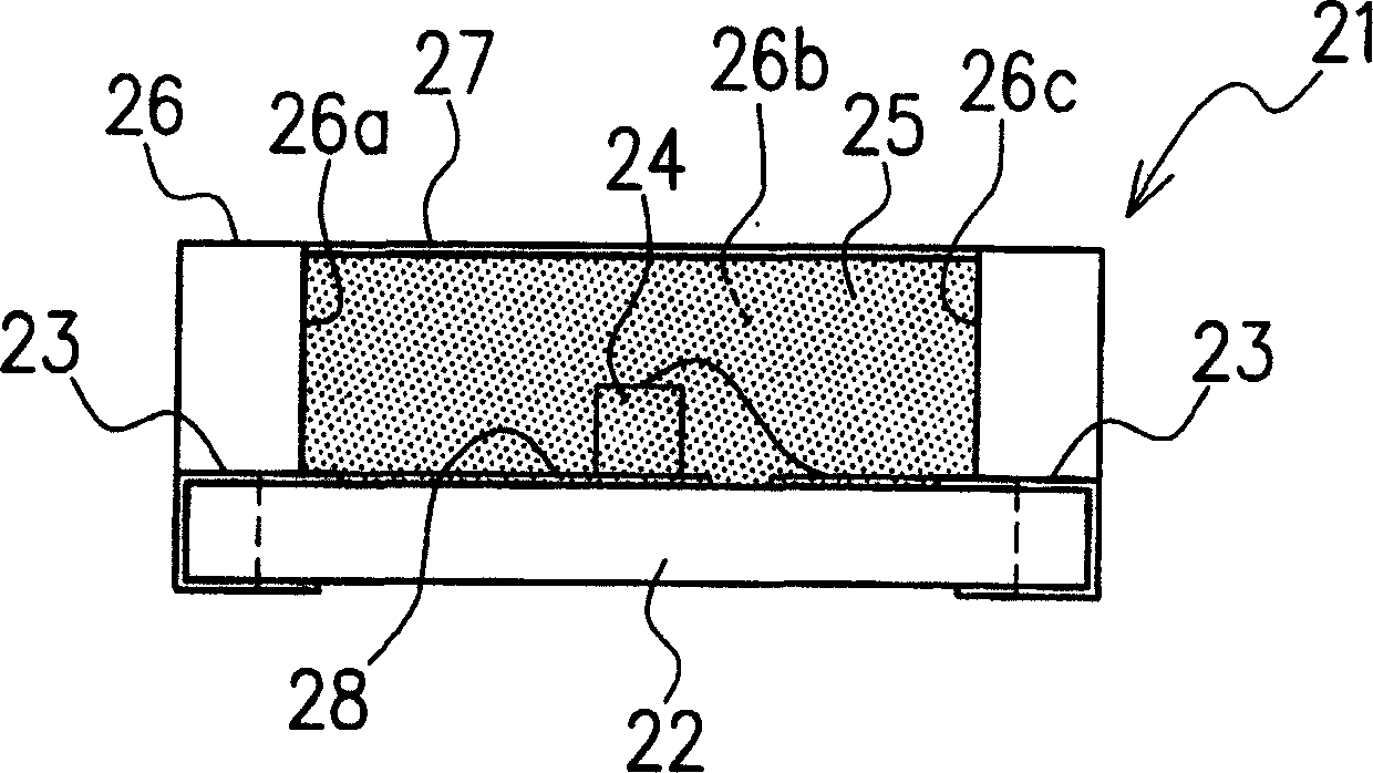
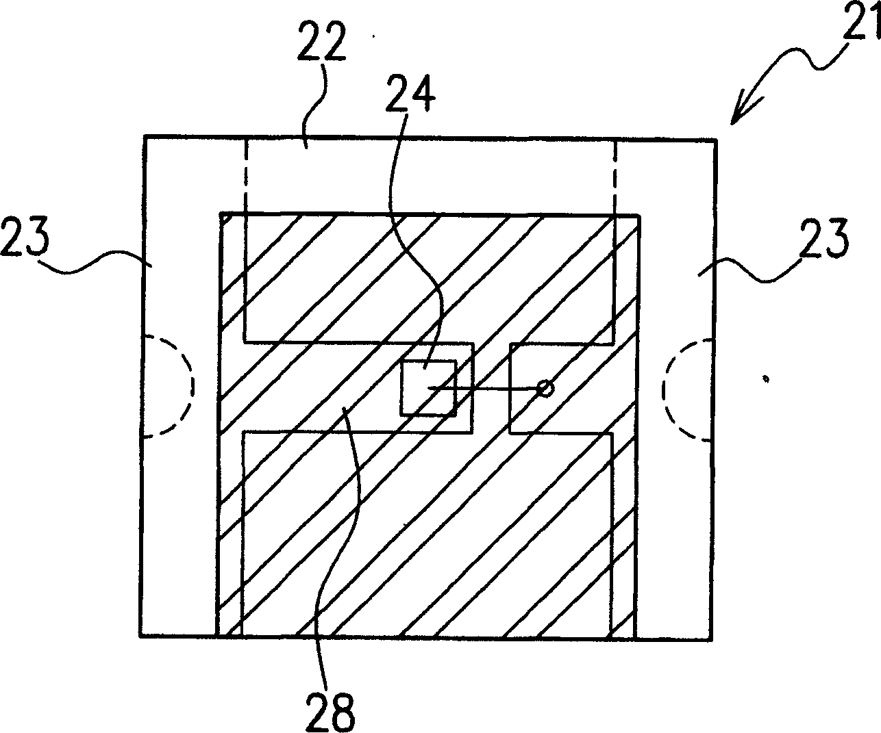
[0024] figure 1 is a perspective view showing a light emitting diode according to the first embodiment of the present invention, figure 2 is a cross-sectional view showing the above light-emitting diode, image 3 is a plan view showing the light emitting diode.
[0025] like Figure 1 to Figure 3 As shown, the light emitting diode 21 of the present invention includes an LED chip (LED chip 24) mounted on a chip substrate 22 formed of glass epoxy resin or BT resin (bismaleimide triazine resin), etc. The LED chip 24 is sealed on a transparent resin body 25 on the chip substrate 22 , a reflective frame 26 surrounding three sides of the transparent resin body 25 , and a reflective film 27 formed on the above-mentioned transparent resin body 25 . And be formed on the three side faces of above-mentioned reflective frame body 26 to be formed with reflective surface 26a, 26b, 26c, make the resin of light-transmitting resin body 25 not surrounded by this reflective surface 26a, 26b,...
Embodiment approach 2
[0032] Figure 4 as well as Figure 5 Shown is the light emitting diode 31 of the second embodiment. The light emitting diode 31 consists of a chip substrate 32 formed with a chip soldering pattern 34 for mounting the LED chip 24 and electrode terminals 33, a reflective frame 36 formed with a recess for sealing the LED chip 24 placed on the chip substrate 32, and a filling. The light-transmitting resin body 35 of the above-mentioned concave portion is constituted. The concave portion is formed in a U-shape, and its inner peripheral surface is a reflection surface 36 a that reflects light emitted from the LED chip 24 . Furthermore, the exposed upper surface of the light-transmitting resin body 35 filled in the recess is formed with the same reflective film 37 as in Embodiment 1, and the exposed portion on one side of the reflective frame 36 is the light exit surface 35a.
[0033] According to the light emitting diode 31 of the above-mentioned structure, the light can be irra...
Embodiment approach 3
[0035] Image 6 as well as Figure 7 Shown is a light emitting diode 41 according to a third embodiment of the present invention. The light emitting diode 41 consists of a triangular chip substrate 42 on which a chip bonding pattern 44 for mounting the LED chip 24 and an electrode terminal 43 are formed, and an L-shaped reflective frame having two reflective surfaces 46a, 46b on both sides of the chip substrate 42. body 46 and the light-transmitting resin body 45 filled and molded in the reflective frame body 46 . Furthermore, the above-mentioned light-transmitting resin body 45 that is filled and molded has the same reflective film 47 as that in Embodiment 1 formed on the exposed upper surface, and the exposed portion on one side of the reflective frame 46 is the light emitting surface 45a.
[0036] In the light-emitting diode 41 according to the above-mentioned structure, the light emitted from the LED chip 24 to the light-emitting surface 45a and the light reflected from th...
PUM
 Abstract
Description
Claims
Application Information
 - R&D
- Intellectual Property
- Life Sciences
- Materials
- Tech Scout
- Unparalleled Data Quality
- Higher Quality Content
- 60% Fewer Hallucinations
Browse by: Latest US Patents, China's latest patents, Technical Efficacy Thesaurus, Application Domain, Technology Topic, Popular Technical Reports.
© 2025 PatSnap. All rights reserved.Legal|Privacy policy|Modern Slavery Act Transparency Statement|Sitemap|About US| Contact US: help@patsnap.com


