
Geminate transistors type PMOS radiation dose meter with difference output

A differential output, radiation dose technology, applied in dosimeters, radiation intensity measurement, material analysis using wave/particle radiation, etc., can solve the problems of decreased compensation effect and non-compensation

Inactive Publication Date: 2005-04-13
XINJIANG TECHN INST OF PHYSICS & CHEM CHINESE ACAD OF SCI
View PDF0 Cites 11 Cited by
  • Summary
  • Abstract
  • Description
  • Claims
  • Application Information

AI Technical Summary

Problems solved by technology

The "zero temperature coefficient point" has an obvious compensation effect on the temperature effect of the PMOS dosimeter, but the "zero temperature coefficient point" will change after the PMOSFET is irradiated, which will reduce the compensation effect; at the same time, the "zero temperature coefficient point" method cannot Compensation for the "annealing effect"

Method used


Image

  • Geminate transistors type PMOS radiation dose meter with difference output
  • Geminate transistors type PMOS radiation dose meter with difference output
  • Geminate transistors type PMOS radiation dose meter with difference output

Examples


Embodiment

[0021] The composition of the dosimeter

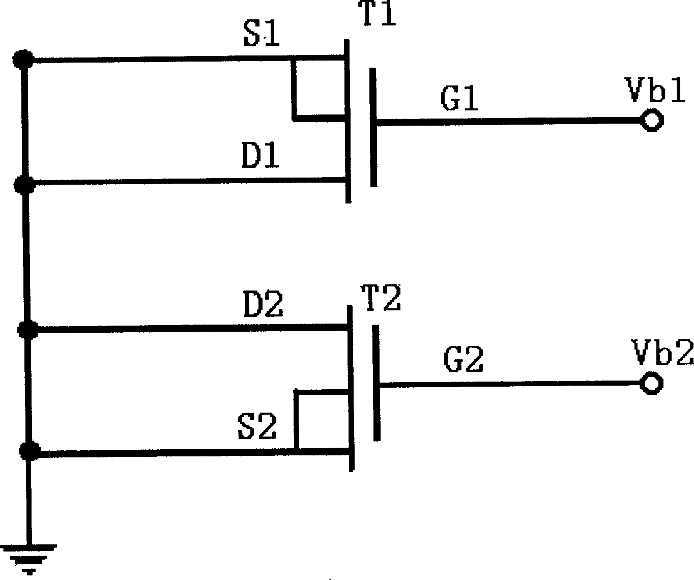
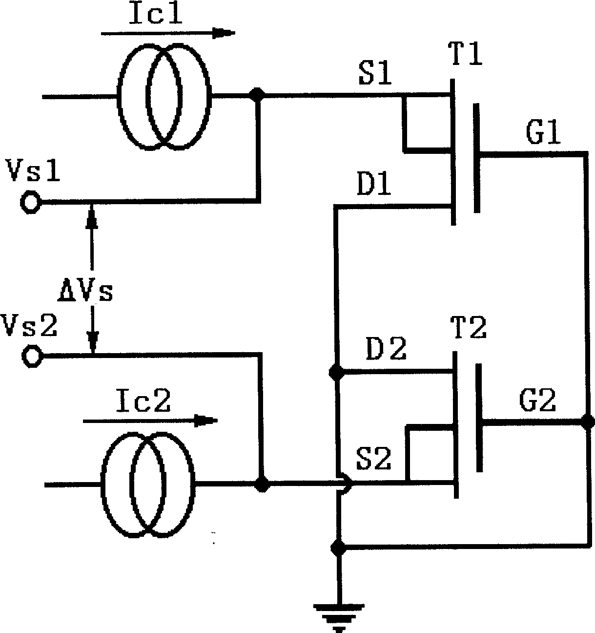
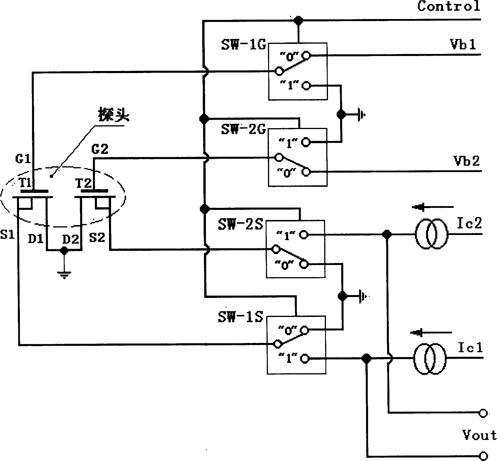
[0022] For tube type differential output PMOS dosimeter, it can be composed of probe, working mode selection switch (SW-1G, SW-2G, SW-1S, SW-2S), DC voltage source (Vb1, Vb2) and constant current source (Ic1, Ic2) Composition; the probe is composed of two identical p-channel field effect transistors T1 and T2; the composition of the probe can be realized in two ways, (1) choose a monolithic device containing two identical pMOSFETs, (2) combine two PMOS monolithic The tubes are installed on a small PCB board as close as possible, and the electrodes of the two tubes are drawn out with lead wires.

[0023] How dosimeters work

[0024] There are two working modes for the tube differential output PMOS dosimeter, one is the measurement mode of receiving and recording the radiation dose; the other is the readout mode of converting the radiation dose record into a voltage signal output.

[0025] In the measurement mode, the sources (S1, S2) ...


PUM


Abstract

The invention discloses a geminate transistors type PMOS radiation dose meter with difference output, wherein the dose meter comprises transistors type PMOS radiation dose meter with difference output and employs measurement offset method, dosage recording and reading technique, temperature compensation process and annealing effect correction method.

Description

technical field [0001] The invention relates to an ionizing radiation dose measurement technology, which relates to the fields of semiconductor physics, solid radiation physics, radiation dosimetry and electronic technology. Background technique [0002] The concept of PMOS dosimeter was first proposed by Holmes-Siedle in England (“The space-charge dosimeter-general principles of a new radiation detection”, Nucl.Instr.Meth.Vol.121, P169-174(1974).) . When a p-channel Metal-Oxide-Semiconductor Transistor (pMOSFET: P channelMetal-Oxide-Semiconductor Transistor) is subjected to ionizing radiation, the threshold voltage of the device will drift with the radiation dose due to the positive charge of the oxide layer and the generation of interface states. For a PMOSFET manufactured by a specific process, the magnitude of the threshold voltage shift and the radiation dose received by the device present an approximately linear monotonic relationship, so the magnitude of the threshol...

Claims


Application Information

Patent Timeline
Patent Type & Authority Applications(China)
IPC IPC(8): G01N23/00G01T1/02G01T1/24
Inventor 郭旗任迪远
Owner XINJIANG TECHN INST OF PHYSICS & CHEM CHINESE ACAD OF SCI
Learn More