Method for mfg. electrostatic discharge protector by deep amicron process

A technology of electrostatic discharge protection and manufacturing method, which is applied in semiconductor/solid-state device manufacturing, circuits, electrical components, etc., can solve the problems of no resistance buffer, no resistance buffer, ESD protection structure damage, etc., to avoid damage Effect

Inactive Publication Date: 2005-03-09
GRACE SEMICON MFG CORP
View PDF0 Cites 4 Cited by
  • Summary
  • Abstract
  • Description
  • Claims
  • Application Information

AI Technical Summary

Problems solved by technology

[0005] However, in deep sub-micron processes, self-aligned metal silicide 22 is applied to polysilicon gate 18 and source / drain regions 24, 16 including electrostatic discharge (ESD) protection structures, such as Figure 4 As shown, this will result in almost no resistive buffer zone between the drain contact 16 and the polysilicon gate 18
When an electrostatic high voltage is generated, causing the parasitic NPN (or PNP) transistor in the ESD protection structure to be triggered, although the current generated by the high voltage can be discharged, the NPN transistor collector N (CollectorN, equivalent to the ggNMOS in ggNMOS Drain) has no resistance buffer zone, coupled with its shallow junction structure design, the flow of high current will be inhomogeneous, resulting in local high current and local heating near the drain, resulting in Potential destruction of the ESD protection structure, thereby losing its role in electrostatic discharge protection

Method used


Image

  • Method for mfg. electrostatic discharge protector by deep amicron process
  • Method for mfg. electrostatic discharge protector by deep amicron process
  • Method for mfg. electrostatic discharge protector by deep amicron process

Examples


Embodiment Construction

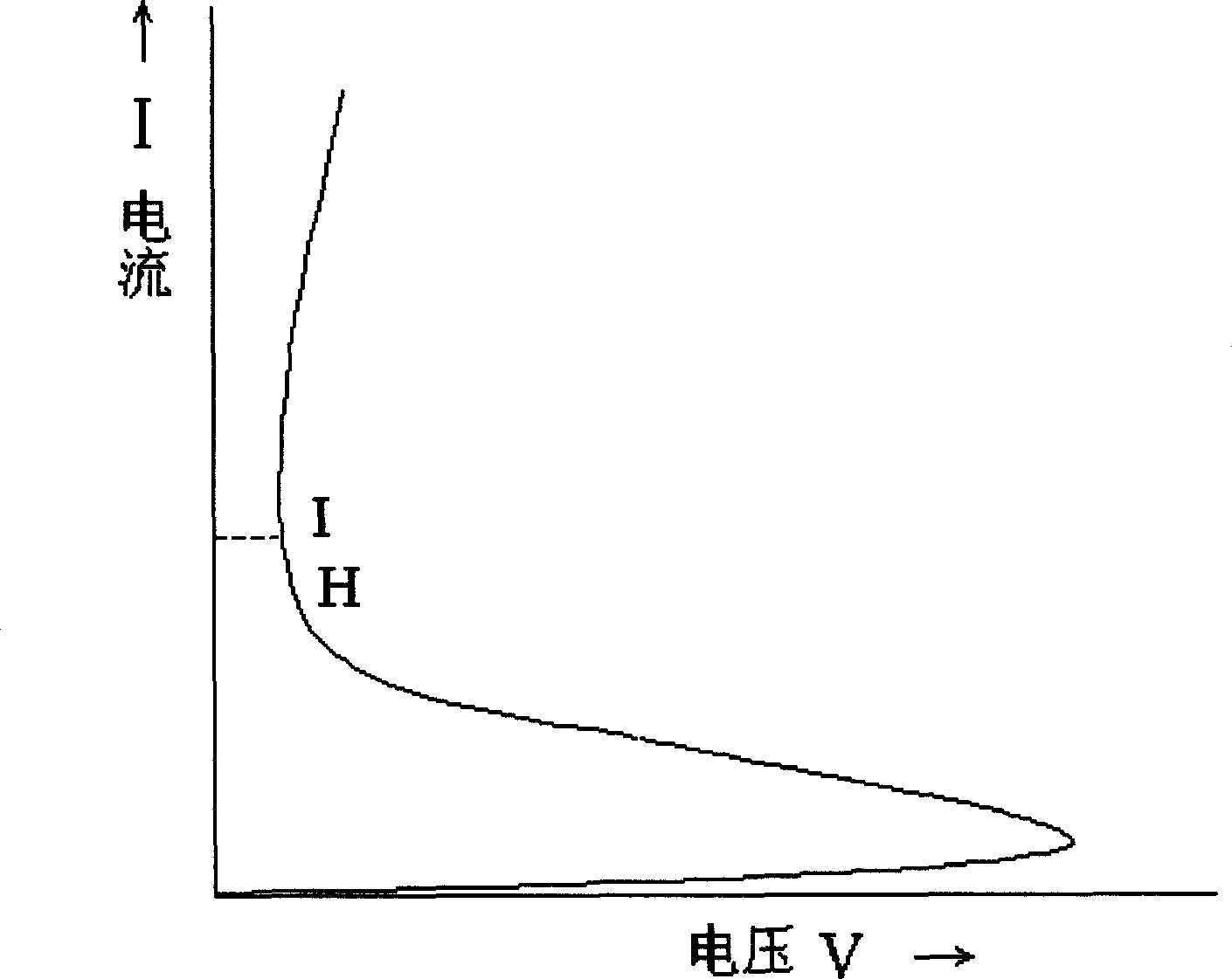
[0027] The invention is used to improve the shortcomings of electrostatic discharge (ESD) protection components in the self-aligned metal silicide process, and adopts the method of self-aligned metal silicide barrier (salicide block) to make the polysilicon gate in the ESD protection component area There is no metal silicide formation on the electrode and source / drain regions, so that there is a resistance ballast between the drain contact (drain contract) and the polysilicon gate (poly gate), which can allow the high current generated by electrostatic discharge It can be removed in a more uniform way, so local high current and local heating will not occur near the drain.

[0028] Figure 5 to Figure 9 They are cross-sectional views of each step of making internal circuits and transistors of the electrostatic discharge protection device in a preferred embodiment of the present invention, taking N-type transistors (NMOS) as an example to describe the manufacturing process of th...


PUM


Abstract

The present invention provides a making method of electrostatic discharge protection device by using deep submicrometer process. Because of that in deep submicrometer process, when the automatic alignment metal silicide is used in transistor source / drain region including electrostatic discharge (ESD) protection component, the nonuniform high current can make the electrostatic protection component be broken, in order to improve said problem, said invention can adopt the automatic alignment metal silicide separation mode to make the electrostatic discharge protection component region have no formation of metal silicide, and make the drain be contacted to a resistance buffer region existed in polycrystalline silicon gate, and can make the high current produced by electrostatic discharge can be removed by utilizing an uniform mode so as to prevent the electrostatic discharge protection structure from being broken.

Description

technical field [0001] The present invention relates to a method for manufacturing an electrostatic discharge protection device (ESD Protection device), in particular to a method for applying self-aligned metal silicide (Self-aligned Silicide, Salicide) in a deep sub-micron process to an electrostatic discharge protection device The manufacturing method, and at the same time avoid the electrostatic discharge structure from being damaged. Background technique [0002] The structure of N-type or P-type transistors (N / P MOS), such as gg (gate-ground) N / PMOS, gc (gate-control) N / PMOS components or other similar structures, is widely used in current Device components for deep sub-micron ESD protection. N / PMOS mainly lies in the component characteristics of its parasitic bipolar transistor (Bipolar). When a momentary high voltage occurs, its parasitic bipolar transistor will be triggered to properly guide the high current generated by its high voltage to the Vss or Vdd terminal ...

Claims


Application Information

Patent Timeline
Patent Type & Authority Applications(China)
IPC IPC(8): H01L21/8238H01L27/02
CPCH01L27/0251H01L21/823835H01L21/823814
Inventor 高荣正
Owner GRACE SEMICON MFG CORP
Why Eureka
Try Eureka