Method of reading image signal from image senser

An image sensor and image signal technology, applied in the direction of image communication, electrical components, etc., can solve the problems of increasing circuit power consumption and area, reducing light-receiving area, incompatibility, etc., and achieving low analog-to-digital conversion rate, area and power. The effect of high power consumption and convenient image processing

Inactive Publication Date: 2005-01-12
TSINGHUA UNIV
View PDF0 Cites 2 Cited by
  • Summary
  • Abstract
  • Description
  • Claims
  • Application Information

AI Technical Summary

Problems solved by technology

The method of multi-analog-to-digital conversion requires many analog-to-digital converters when the circuit is implemented, which not only increases the power consumption and area of ​​the circuit, but also increases the cost
At the same time, due to the increase of other areas of the circuit, the light-receiving area of ​​each pixel will inevitably be reduced, which will greatly reduce the sensitivity of the CMOS image sensor and affect the quality of image acquisition.
Obviously, the shortcomings of this method are not suitable for the development of modern CMOS large-scale and VLSI towards high-speed and low-power consumption, especially for various mobile electronic devices, such as visual communication mobile phones, various cameras, etc.

Method used


Image

  • Method of reading image signal from image senser
  • Method of reading image signal from image senser
  • Method of reading image signal from image senser

Examples


Embodiment Construction

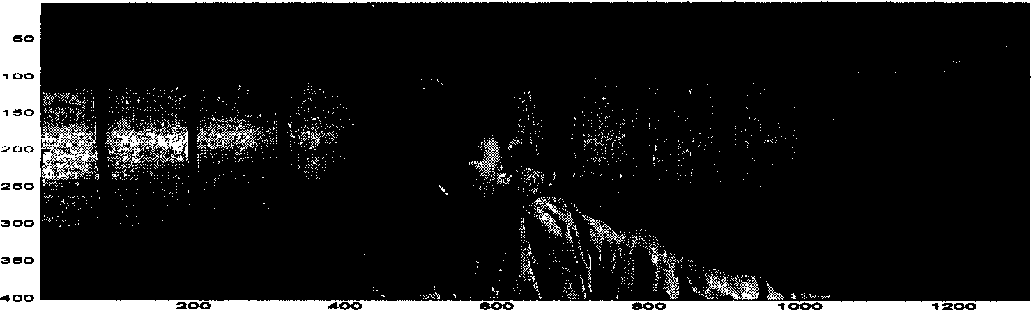
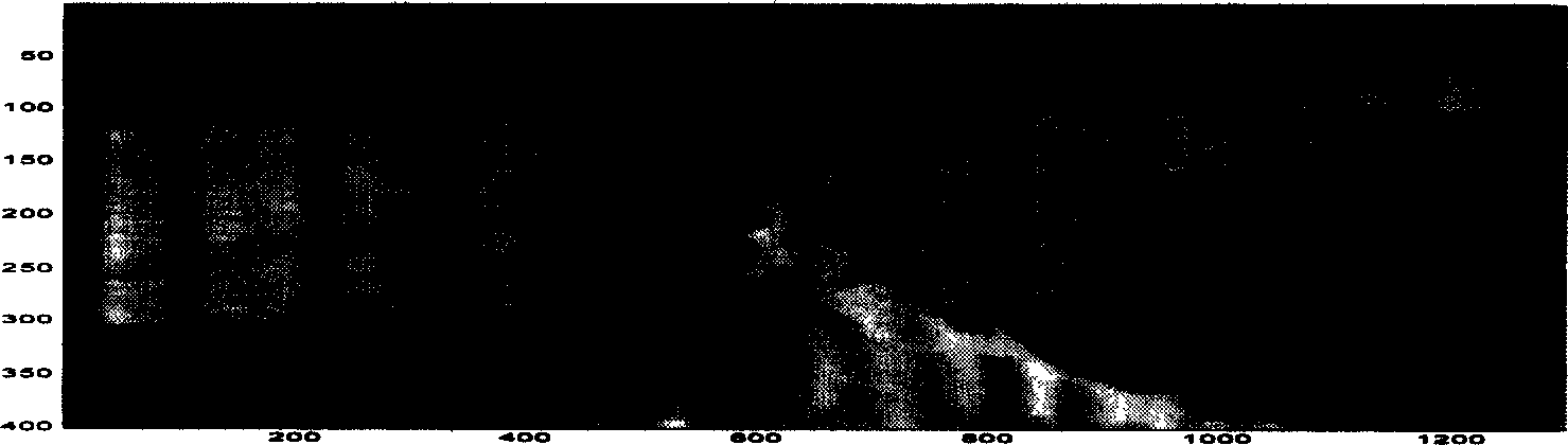
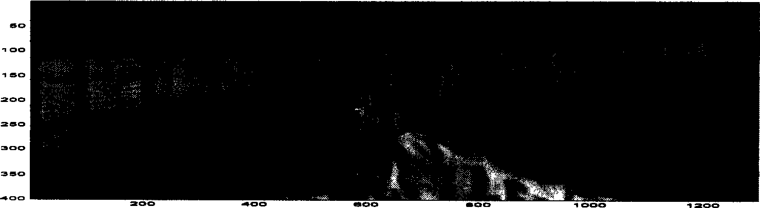
[0010] The readout method of the image signal in the image sensor that the present invention proposes, at first selects the scanning row from the image successively, scans each column pixel successively to the selected scanning row by column scanning frequency; Low-pass filtering of Wn; the analog-to-digital conversion is performed on the low-pass filtered signal to obtain a digital image signal.

[0011] In the above readout method, in order to simplify the subsequent image compression process, the acquisition speed of the image is required to be very high, so the number of images acquired per second is very large, so the high-resolution CMOS image sensor must be very demanding. Row and column scan speed, where the column scan speed is the horizontal resolution times the row scan speed. If a CMOS image sensor with a resolution of 1000×1000 acquires 1000 pictures per second, the row scanning frequency is 1MHz, while the column scanning frequency is as high as 1000MHz. Such a ...


PUM


Abstract

The method first selects up the scan line in turn frmo image, the selected scan line scans each pixel at column scan frequency; the low pass filter whose cut-off frequency is Wn is made for each column pixel; the A/D conversion is made for the signal filtered with low pass filter. By using the invention, the cut-off frequency-Wn is much lower than column scan frequency, the frequency of A/D conversion also much lower than column scan frequency, so that the circuit can implement a high speed image acquisition with a low speed A/D conversion.

Description

technical field [0001] The invention relates to a method for reading out image signals of an image sensor and a circuit thereof, and belongs to the technical field of complementary metal oxide semiconductor (hereinafter referred to as CMOS) image sensors. Background technique [0002] The CMOS image sensor obtains a complete image by scanning and reading out the brightness information of each pixel. In the existing CMOS image sensor, the image signal is obtained by scanning the pixels in rows and columns, and then performing analog-to-digital conversion on the scanned pixel signal. With the improvement of the resolution and image acquisition speed of CMOS image sensors, the traditional readout method requires high-frequency analog-to-digital conversion, that is, an analog-to-digital converter with a high sampling frequency is required for circuit implementation. In order to reduce the frequency of A / D conversion, there are many methods to simultaneously perform A / D conversi...

Claims


Application Information

Patent Timeline
Patent Type & Authority Applications(China)
IPC IPC(8): H04N1/028
Inventor 李金城杨华中罗嵘汪蕙
Owner TSINGHUA UNIV
Why Eureka
Try Eureka