Film optical addressing electric potential sensor used for detecting Fe3+ and preparation method thereof

A potentiometric sensor and optical addressing technology, applied in instruments, measuring devices, scientific instruments, etc., can solve the problems of complex pretreatment, long measurement period, huge equipment, etc. Effect

Inactive Publication Date: 2004-11-17
ZHEJIANG UNIV
View PDF0 Cites 5 Cited by
  • Summary
  • Abstract
  • Description
  • Claims
  • Application Information

AI Technical Summary

Problems solved by technology

The current detection methods mainly include atomic absorption spectrophotometry and mass spectrometry, etc., but the equipment used in these methods is huge and e

Method used


Image

  • Film optical addressing electric potential sensor used for detecting Fe3+ and preparation method thereof
  • Film optical addressing electric potential sensor used for detecting Fe3+ and preparation method thereof
  • Film optical addressing electric potential sensor used for detecting Fe3+ and preparation method thereof

Examples


Embodiment Construction

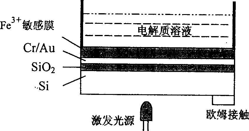
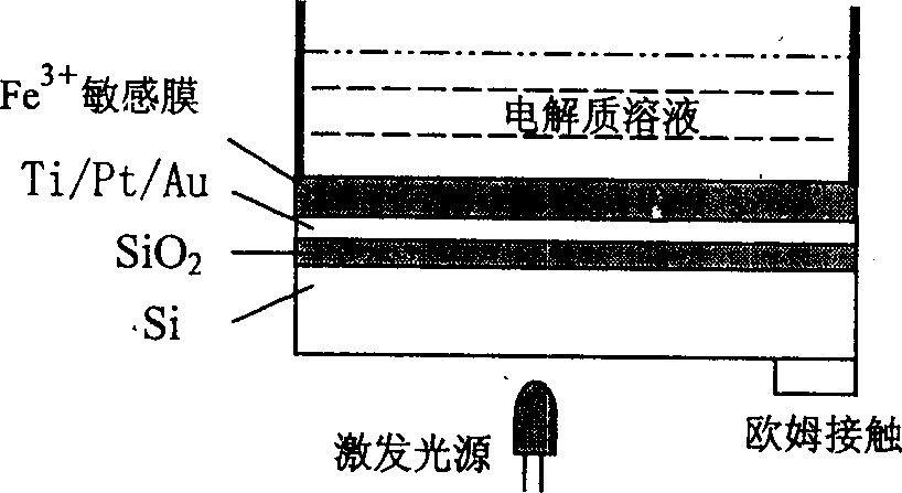
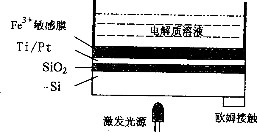
[0024] Structure of the sensor

[0025] Use p-type or n-type Si sheets as the substrate, and there are SiO on the substrate from bottom to top. 2 layer, metal layer, for Fe 3+ sensitive film. The metal layer is Cr as the lower layer and Au as the upper layer, such as figure 1 shown; or the lower layer is Ti, the middle layer is Pt, and the upper layer is Au, such as figure 2 shown; or the lower layer is Ti, the upper layer is Pt, such as image 3 As shown; the excitation light source can be front or back lighting.

[0026] Preparation of sensors

[0027] (1) Preparation of LAPS

[0028] A p-type or n-type monocrystalline silicon wafer is selected as the substrate of LAPS. After the silicon wafer is polished and cleaned, it is placed in a high-temperature furnace for thermal oxidation, so that a layer of SiO with a thickness of about 30nm is grown on the front of the silicon wafer in dry oxygen. 2 Remove the oxide layer on the back of the silicon wafer by ion etching,...


PUM

PropertyMeasurementUnit
Thicknessaaaaaaaaaa

Abstract

The invention discloses film light addressing potential sensor for measuring Fe3+ and the manufacturing method. The sensor is based on the light addressing potential sensor (LAPS), a layer of sensitive film is produced on its surface with laser pulse depositing technology. The invention synthesizes the sensitive material at first, which is used as the target of pulse laser deposition. Then it produces a fixed metal layer through magnetism control sputtering technology on LAPS, and then carries on the process of film with laser pulse depositing technology and device. The film sensor is sensitive to the Fe3+ in the liquid; it can detect the content of Fe3+.

Description

Technical field [0001] The invention relates to a method for detecting Fe 3+ Thin film photoaddressable potentiometric sensor and its preparation method. Background technique [0002] Heavy metal ions (such as Zn 2+ , Pb 2+ 、Cd 2+ 、Cu 2+ 、Cr 6+ , Mn 5+ 、As 3+ , Fe 3+ , Hg 2+ ) can have harmful or even fatal effects on the human body, so the quantitative detection of heavy metals is of great significance in medicine, food, clinical and environmental monitoring. The current detection methods mainly include atomic absorption spectrophotometry and mass spectrometry, etc., but the equipment used in these methods is huge and expensive, requires complex pretreatment, long measurement period and skilled operators, which brings great problems in practical applications. Many inconveniences. Contents of the invention [0003] The object of the present invention is to provide a method for detecting Fe 3+ Thin-film light-addressable potential sensor and preparation method t...

Claims


Application Information

Patent Timeline
IPC IPC(8): G01N27/333
Inventor 王平门洪李毅许祝安
Owner ZHEJIANG UNIV
Why Eureka
Try Eureka