Array filmsensor for simultaneously detecting Cu2+, Pb2+, Cd2+ and its preparing method
A thin-film sensor and array technology, applied in instruments, measuring devices, scientific instruments, etc., can solve the problems of long measurement cycle, complex pretreatment, and huge equipment, and achieve the effects of fast measurement, less sample solution, and convenient use.
- Summary
- Abstract
- Description
- Claims
- Application Information
AI Technical Summary
Problems solved by technology
Method used
Image

Examples
Embodiment 1
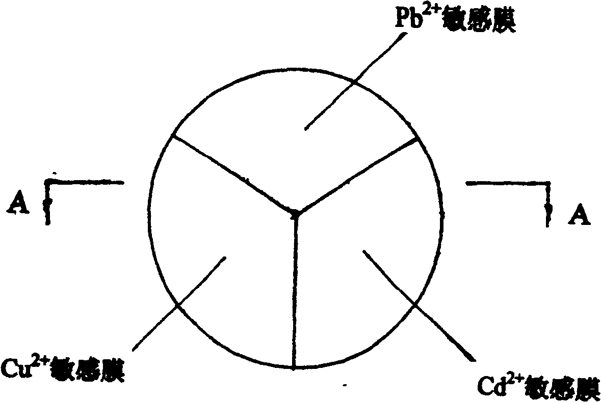
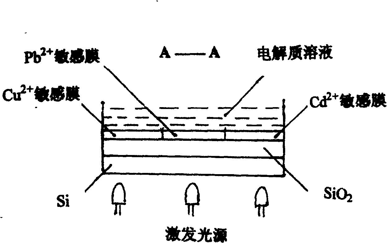
[0025] From figure 2 and figure 1 It can be seen that the present invention is used for simultaneous detection of Cu 2+ , Pb 2+ 、Cd 2+ The array thin-film sensor of the company uses p-type or n-type Si sheets as the substrate, and SiO2 is placed on the substrate. 2 layer, SiO 2 There are three kinds of layers above Cu 2+ , Pb 2+ 、Cd 2+ sensitive film.
[0026] The invention is used for simultaneous detection of Cu 2+ , Pb 2+ 、Cd 2+ The preparation of the arrayed thin film sensor consists of the following steps:
[0027] (1) Preparation of thin film sensor substrate and oxide layer
[0028] A p-type or n-type monocrystalline silicon wafer is selected as the substrate. After the silicon wafer is polished and cleaned, it is placed in a high-temperature furnace for thermal oxidation, so that a layer of SiO with a thickness of about 30nm is grown on the front of the silicon wafer in dry oxygen. 2 Remove the oxide layer on the back of the silicon wafer by ion etching...
Embodiment 2
[0036] (1) Preparation of thin film sensor substrate and oxide layer
[0037] A p-type or n-type monocrystalline silicon wafer is selected as the substrate. After the silicon wafer is polished and cleaned, it is placed in a high-temperature furnace for thermal oxidation, so that a layer of SiO with a thickness of about 30nm is grown on the front of the silicon wafer in dry oxygen. 2 Remove the oxide layer on the back of the silicon wafer by ion etching, and then use silver paste to make a ring-shaped ohmic contact lead-out wire. Except for the ring-shaped part, the rest are sealed with epoxy resin, which is the finished product. For the thin-film sensor substrate described above, the excitation light source can be either the front or the back;
[0038] (2) Preparation of sensitive materials
[0039] Selection of high-purity compounds CuS, Ag 2 S, CuI 2 , its molar ratio is 60: 25: 15. After fully leaking and grinding, under the pressure of 12Mpa, make a small cuboid, put ...
Embodiment 3
[0045] (1) Preparation of thin film sensor substrate and oxide layer
[0046] A p-type or n-type monocrystalline silicon wafer is selected as the substrate. After the silicon wafer is polished and cleaned, it is placed in a high-temperature furnace for thermal oxidation, so that a layer of SiO with a thickness of about 30nm is grown on the front of the silicon wafer in dry oxygen. 2 Remove the oxide layer on the back of the silicon wafer by ion etching, and then use silver paste to make a ring-shaped ohmic contact lead-out wire. Except for the ring-shaped part, the rest are sealed with epoxy resin, which is the finished product. For the thin-film sensor substrate described above, the excitation light source can be either the front or the back;
[0047] (2) Preparation of sensitive materials
[0048] Selection of high-purity compounds CuS, Ag 2 S, CuI 2 , the molar ratio of which is 65:30:20, after fully mixing and grinding, under the pressure of 12Mpa, make a small cuboid...
PUM
| Property | Measurement | Unit |
|---|---|---|
| thickness | aaaaa | aaaaa |
| diameter | aaaaa | aaaaa |
| thickness | aaaaa | aaaaa |
Abstract
Description
Claims
Application Information
 - R&D
- Intellectual Property
- Life Sciences
- Materials
- Tech Scout
- Unparalleled Data Quality
- Higher Quality Content
- 60% Fewer Hallucinations
Browse by: Latest US Patents, China's latest patents, Technical Efficacy Thesaurus, Application Domain, Technology Topic, Popular Technical Reports.
© 2025 PatSnap. All rights reserved.Legal|Privacy policy|Modern Slavery Act Transparency Statement|Sitemap|About US| Contact US: help@patsnap.com