Method for making nano device

A technology of nano-devices and electron beam exposure, which is applied in nanotechnology, nanotechnology, nanostructure manufacturing, etc., and can solve problems such as long exposure time

Inactive Publication Date: 2004-10-13
SEMICON MFG INT (SHANGHAI) CORP +1
View PDF0 Cites 9 Cited by
  • Summary
  • Abstract
  • Description
  • Claims
  • Application Information

AI Technical Summary

Problems solved by technology

However, since the electron beam exposure system usually uses a thinner beam spot for ultra-fine graphic scanning exposure, the higher the graphic accuracy requirement, the finer the beam spot required for drawing the graphic, and the smaller the corresponding beam current density. Sensitivity conditions require longer exposure times

Method used


Image

  • Method for making nano device
  • Method for making nano device
  • Method for making nano device

Examples


Embodiment Construction

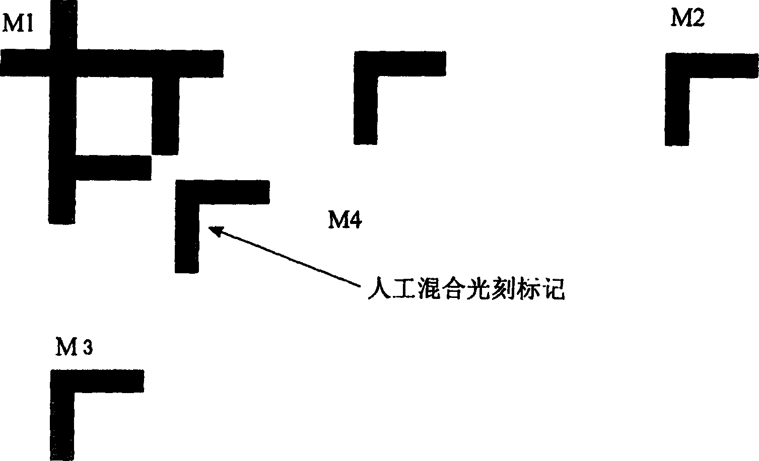
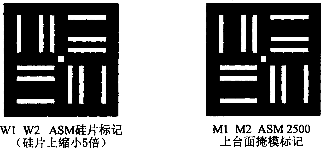
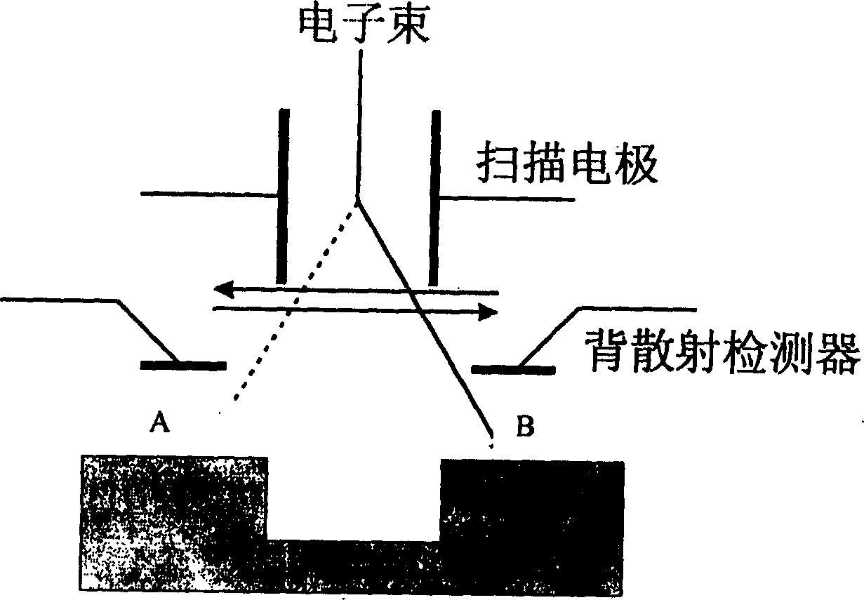
[0032] A kind of method for manufacturing nano-device of the present invention is characterized in that, comprises the following steps:

[0033] (1) Prepare an overlay detection mark mask for electron beam and optical exposure machines;

[0034] (2) substrate is coated with PMMA resist, and its glue thickness is 450-500nm;

[0035] (3) pre-baking, the temperature is 165 ℃, and the time is 40 seconds;

[0036] (4) Electron beam exposure, the accelerating voltage is 50KV, the dose is 380uC / cm 2 , the beam current is 2nA, and the edge characteristics of the marked pattern exposed by the electron beam are good;

[0037] (5) developing MIBK:IPA=1:3, the time is 1 minute, and then fixed in IPA solution for 30 seconds;

[0038] (6) Evaporating or sputtering metal, the thickness of which is 250nm;

[0039] (7) peel off in acetone solution;

[0040] (8) The electron beam resist (PMMA) is coated for the second time, and the glue thickness is 200-250nm;

[0041] (9) Pre-baking;

...


PUM

PropertyMeasurementUnit
thicknessaaaaaaaaaa

Abstract

The present invention relates to a method for making nano device. The method includes the following steps: preparing overlay detection mark mask plate of electron-beam and optical exposure machine; applying PMMA resist on substrate, prebaking, electron-beam exposure, developing MIBK:IPA=1:3, time is 1 min, fixing for 30 sec. in IPA solution, evaporation or sputtering metal, stripping in acetone solution, applying secondary electron-beam resist, thickness is 200-250 nm, prebaking, utilizing the method for detecting back scattered electron of mark edge by using electron-beam to detect whole mark on the substrate and small mark of every die, correcting according to measured value, secondary electron-beam exposure, accelerating voltage 50KV, dose 500 u C / sq.cm, beam current 100 Pa, developing MIBK:IPA=1:3, time is 1 min, fixing for 30 sec in IPA solution, optically exposing other pattern for making device, finally forming nano-grade device.

Description

technical field [0001] The invention provides a method for manufacturing a nanometer device, in particular a method for manufacturing a nanometer device by using a microfabrication method (different from a self-assembly method). Background technique [0002] Due to its high efficiency, optical exposure is the mainstream technology of integrated circuit manufacturing at present, but the resolution of optical exposure is limited by the exposure wavelength and can reach nanoscale resolution. Electron beam exposure has a very high resolution, and the resolution of high-performance electron beam exposure machines can reach several nanometers. However, since the electron beam exposure system usually uses a thinner beam spot for ultra-fine graphic scanning exposure, the higher the graphic accuracy requirement, the finer the beam spot required for drawing the graphic, and the smaller the corresponding beam current density. The higher the sensitivity, the longer the exposure time is...

Claims


Application Information

Patent Timeline
Patent Type & Authority Applications(China)
IPC IPC(8): B82B3/00
Inventor 刘明陈宝钦徐秋霞郑英葵
Owner SEMICON MFG INT (SHANGHAI) CORP
Why Eureka
Try Eureka