CCD image sensor
A charge-coupled device, image sensor technology, used in electrical components, image communications, components of TV systems, etc., can solve problems such as inability to arrange photodiodes, lowering potential, and narrow paths.
- Summary
- Abstract
- Description
- Claims
- Application Information
AI Technical Summary
Problems solved by technology
Method used
Image
Examples
no. 1 example
[0090] Figure 7 is a plan view of the CCD image sensor according to the first embodiment of the present invention.
[0091] The illustrated CCD image sensor 100A includes first to fourth rows of charge transfer devices 101a, 101b, 101c, and 101d, first and second rows of photodiodes 102a and 102b, first to fourth rows of charge transfer devices 101a, 101b, 101c and 101d are connected in common to output gate 103, reset gate 104, drain 105, charge detection capacitor 106 including a floating source and source output circuit 107 serving as a charge detector.
[0092] The first to fourth charge transfer devices 101a, 101b, 101c, and 101d are structurally identical to each other, and the first and second photodiodes 102a and 102b are structurally identical to each other. The charge reading gate 110 is disposed between each of the first to fourth charge transfer devices 101a, 101b, 101c and 101d and each of the first and second photodiodes 102a and 102b. Each of the first and se...
no. 2 example
[0127] Figure 15 is in the CCD image sensor according to the second embodiment of the present invention, and Figure 7 Shown is an enlarged plan view of the area corresponding to area A, while Figure 16 is in the area Figure 15 A floor plan of the lower level below the portion described.
[0128] The CCD image sensor 100B according to the second embodiment is structurally different from the CCD image sensor 100A in the shape of the output gate 103 and the shape of the n-type well 113 located below the output gate 103 .
[0129] In the first embodiment, as Figure 12 As shown, in the layer located below the output gate 103, p + The channel stopper 115 extends to the region immediately below the gate electrode 103b, while in the region directed to the charge detection capacitor 106, the width of the n-type well 113 of the charge transfer devices 101b and 101c is narrowed. Therefore, in this region, p + The proximity of the diffusion layers to each other results in a pot...
no. 3 example
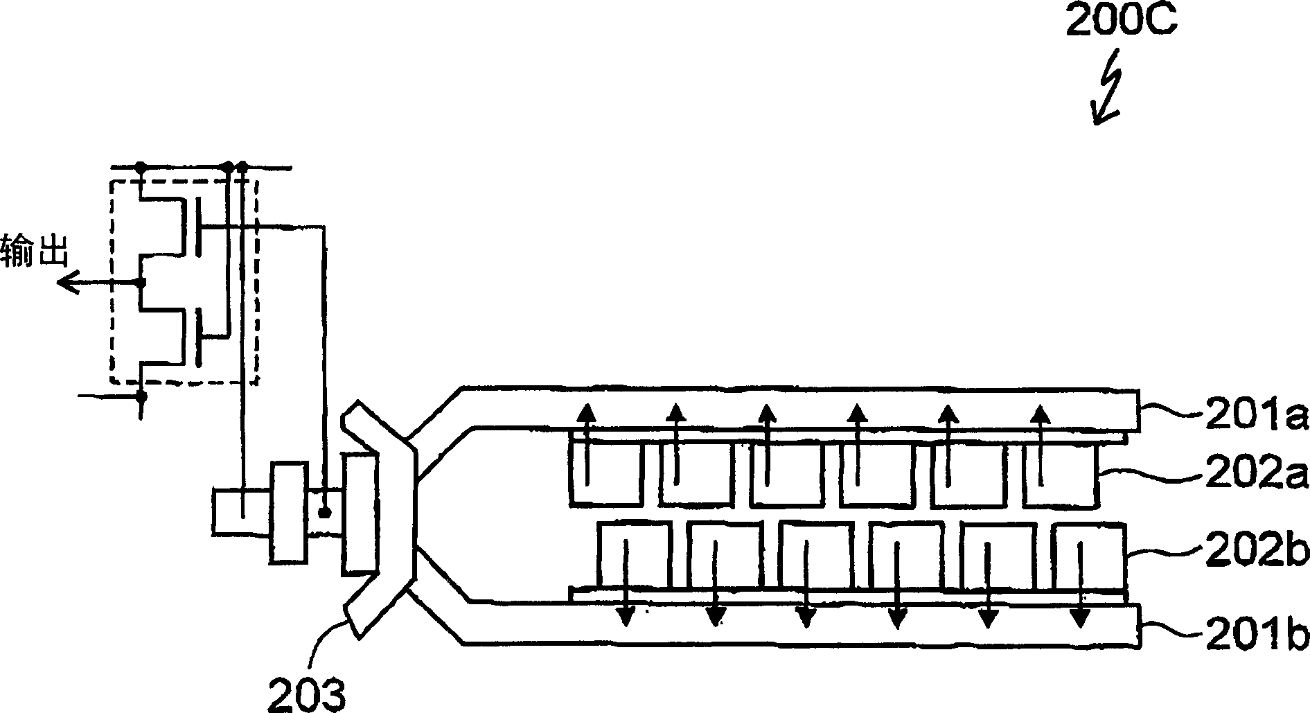
[0139] Figure 17 is a plan view of a CCD image sensor according to a third embodiment of the present invention.
[0140] A CCD image sensor 100C according to the third embodiment is structurally different from the CCD image sensors 100A and 100B according to the first and second embodiments in that the CCD image sensor 100C includes one row of charge transfer devices 101f instead of two rows of charge transfer devices 101b and 101c, and input the charge transferred by any one of the three rows of charge transfer devices 101a, 101d, and 101f into the charge detection capacitor 106.
[0141] For example, the photodiodes in the first and second photodiode rows 102a and 102b emit charge in the directions indicated by the arrows. The four rows of charge transfer devices in the CCD image sensors 100A and 100B can be replaced with the same three rows of charge transfer devices as in the third embodiment.
PUM
 Abstract
Description
Claims
Application Information
 - R&D
- Intellectual Property
- Life Sciences
- Materials
- Tech Scout
- Unparalleled Data Quality
- Higher Quality Content
- 60% Fewer Hallucinations
Browse by: Latest US Patents, China's latest patents, Technical Efficacy Thesaurus, Application Domain, Technology Topic, Popular Technical Reports.
© 2025 PatSnap. All rights reserved.Legal|Privacy policy|Modern Slavery Act Transparency Statement|Sitemap|About US| Contact US: help@patsnap.com


