Semiconductor laser butterfly packaging device

A technology for packaging devices and lasers, applied in the field of semiconductor and optical fiber communication, can solve the problems of no light output, difficult coupling and alignment, low production efficiency, etc., achieve high-frequency characteristics and good temperature stability, reduce production costs, and improve production. The effect of efficiency

Inactive Publication Date: 2004-03-03
INST OF SEMICONDUCTORS - CHINESE ACAD OF SCI
View PDF0 Cites 5 Cited by
  • Summary
  • Abstract
  • Description
  • Claims
  • Application Information

AI Technical Summary

Problems solved by technology

In the common semiconductor laser butterfly packaging device, the optical fiber is usually fixed on the pedestal of the butterfly shell or in the tail pipe attached to the shell by laser welding or gluing. This coupling method has difficulties in coupling and alignment. It is necessary to precisely adjust the optical fiber to the light-emitting position of the semiconductor laser, resulting in low production efficiency, high requirements for skilled workers, and high production costs; and during the working process of the semiconductor laser butterfly packaging device, due to the heating of the semiconductor laser itself, The heat migration effect of the semiconductor refrigerator, the temperature change of the surrounding environment and other reasons will cause a certain temperature gradient between the position of the semiconductor laser and the position of the fixed optical fiber, so that the thermal expansion and contraction of the material are not consistent, which will eventually lead to the position of the semiconductor laser. The position relative to the optical fiber changes, which affects the light output stability of the device. In severe cases, there may even be no light output at all.

Method used


Image

  • Semiconductor laser butterfly packaging device
  • Semiconductor laser butterfly packaging device
  • Semiconductor laser butterfly packaging device

Examples


Embodiment Construction

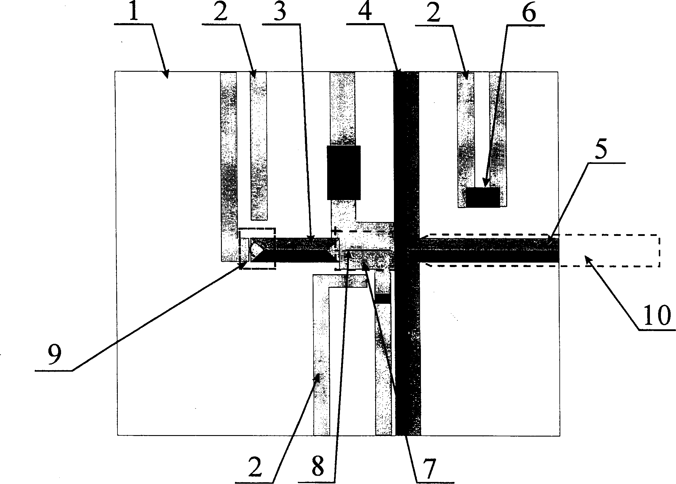
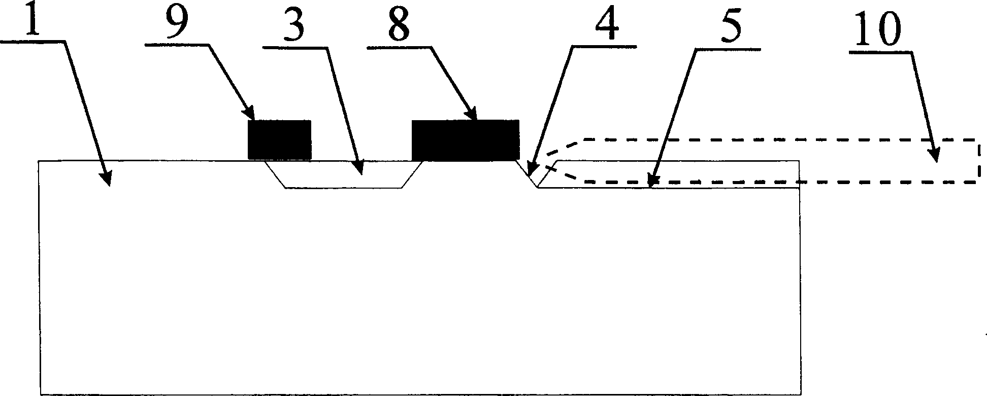
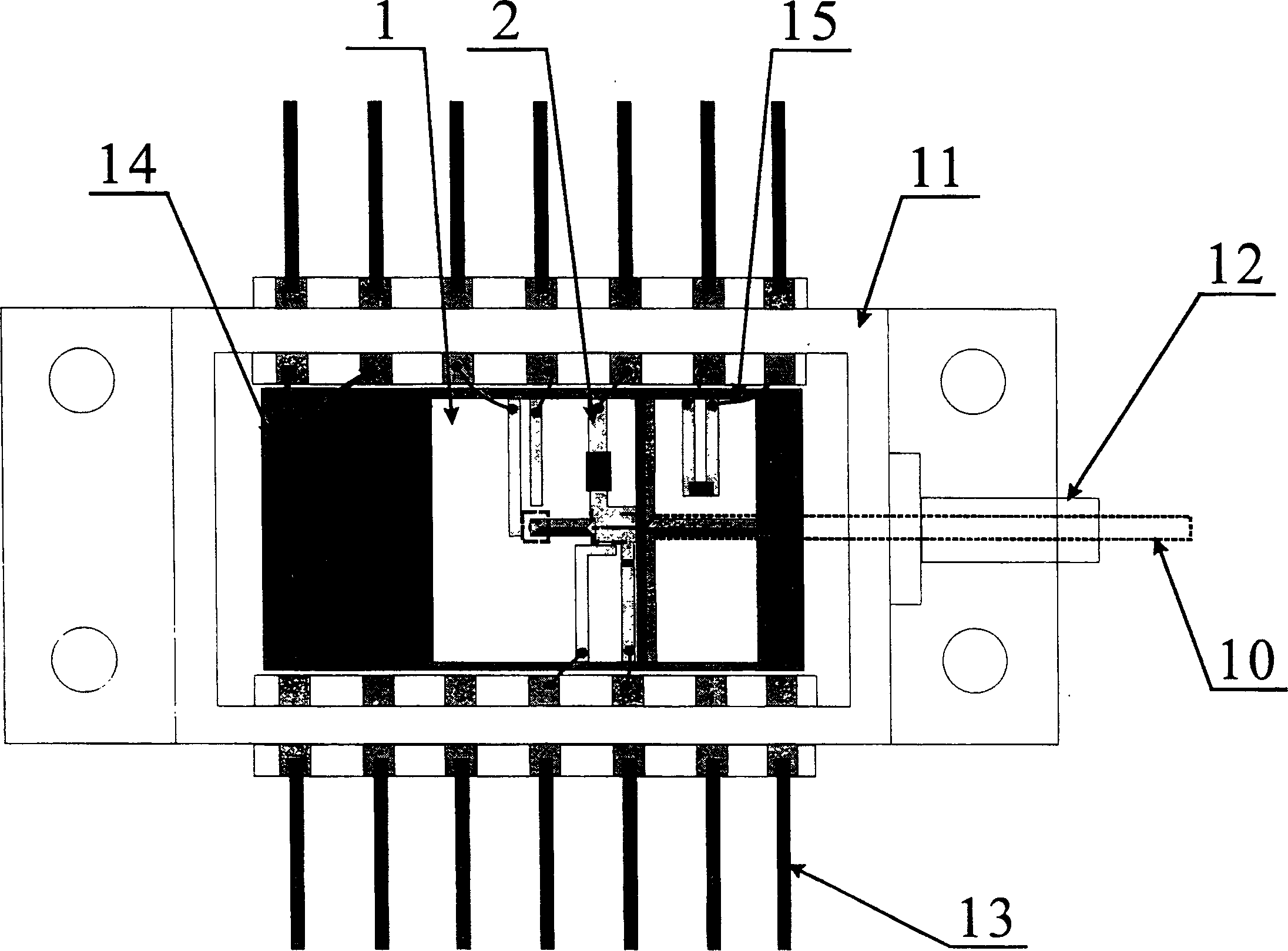
[0015] exist figure 1 and figure 2 In the embodiment, the V-groove 5 for the optical fiber, the V-groove 4 for the longitudinal direction and the V-groove 3 for the backlight are respectively made on the silicon heat sink 1 by wet etching micromachining technology. Then microelectronics technology is used to form a microwave microstrip circuit 2 and an alignment mark 8 on the silicon heat sink 1 , and to form a back gold layer on the back of the silicon heat sink 1 . During this process, it is easy to ensure strict alignment with the center line of the optical fiber V-groove 5 and the alignment mark 8 by utilizing the precision of the micro-machining technology and the micro-electronics process. Align the waveguide and cleavage plane of the semiconductor laser 7 with the corresponding mark of the alignment mark 8 by using an upside-down welding machine, and weld them on the microwave microstrip circuit 2 . The head of the optical fiber 10 is shaped into a conical shape by g...


PUM


Abstract

A butterfly-shaped package of semiconductor laser is composed of a butterfly-shaped case, a semiconductor refrigerator, and a thermal silicon sink on which there are semiconductor laser device, optical fibre, back light detector and microwave microstrip circuit. Its advantages are high HF characteristics and temp stability, and low cost.

Description

technical field [0001] The invention belongs to the technical field of semiconductor and optical fiber communication, more specifically, it belongs to a butterfly package coupling device of a semiconductor laser and an optical fiber. Background technique [0002] In optical fiber communication technology, semiconductor lasers are usually used as signal sources for optical fiber communication. In order to guide the laser light generated by the semiconductor laser into the optical fiber, it is necessary to couple and package the semiconductor laser into a specific packaging form to achieve stable and reliable coupling of the optical signal generated by the semiconductor laser into the optical fiber, and DC bias, modulation The purpose of introducing electrical signals such as signals into semiconductor lasers. Common coupling package forms include coaxial package, butterfly package, dual in-line package, small dual in-line package and so on. Among them, the butterfly package...

Claims


Application Information

Patent Timeline
Patent Type & Authority Applications(China)
IPC IPC(8): G02B6/42H01S5/00
Inventor 陈振宇祝宁华
Owner INST OF SEMICONDUCTORS - CHINESE ACAD OF SCI
Why Eureka
Try Eureka