Electronic cyclotron resonance dusting device for treatment of glass chip or chip

A technology for processing objects and ash chambers, which is applied in the photoengraving process of circuits, electrical components, and pattern surfaces, etc., and can solve the problems of small plasma area and difficult to large substrates.

Inactive Publication Date: 2002-04-03
DMS CO LTD
View PDF0 Cites 5 Cited by
  • Summary
  • Abstract
  • Description
  • Claims
  • Application Information

AI Technical Summary

Problems solved by technology

However, there is such a problem that in the above-mentioned conventional ECR deashing apparatus, the area to be irradiated with plasma is small, so it is difficult to apply to a case with a large substrate.

Method used


Image

  • Electronic cyclotron resonance dusting device for treatment of glass chip or chip
  • Electronic cyclotron resonance dusting device for treatment of glass chip or chip
  • Electronic cyclotron resonance dusting device for treatment of glass chip or chip

Examples


Embodiment Construction

[0020] The present invention will now be described in detail with reference to the accompanying drawings.

[0021] In the following description, the production of wafers in semiconductor devices is considered to be the same thing as the production of glass substrates in liquid crystal displays, so that the ECR ash removal apparatus for processing wafers will not be described.

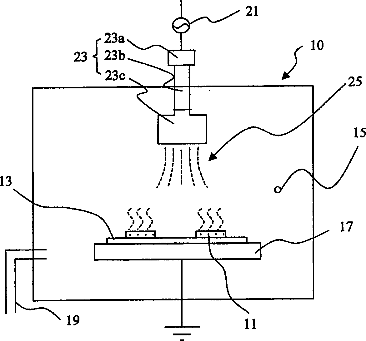
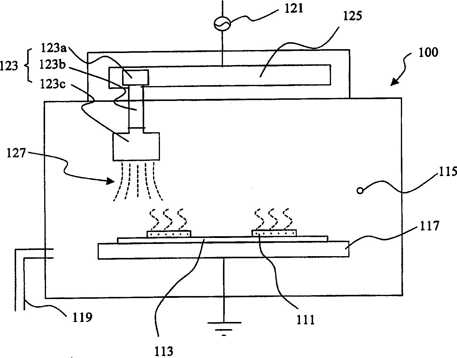
[0022] figure 2 The ECR ash removal device for liquid crystal display glass substrate according to the present invention is schematically shown. Such as figure 2 As shown, the ECR ash removal device of the present invention includes: ash removal chamber 100, an insertion port (not shown) of a glass substrate, an exhaust port 119 of ash removal gas and an air supply part 115 are provided on one side thereof; Electrode 117, in the deashing chamber 100, glass substrate 113 is installed on the lower electrode 117, wherein photoresist material 111 is applied on the glass substrate; RF power supply (not s...


PUM


Abstract

An electron cyclotron ashing device is provided with an ashing chamber having a glass substrate or wafer pulling-in port, an ashing gas discharging port, and a gas supplying section on one side, a lower electrode on which the glass substrate or wafer coated with a photoresist is stably placed in the ashing chamber, and an RF power source which supplies electric power to the lower electrode. The ashing device is also provided with the ECR source which forms a plasma in the ashing chamber, an electric power supplying device which supplies electric power to the ECR source, a scanning device which drives the ECR source or glass substrate or wafer facing the source forward and backward or leftward and rightward, and others.

Description

technical field [0001] The present invention relates to an apparatus for producing semiconductor devices, and in particular, to an electron cyclotron resonance (hereinafter referred to as ECR) deashing apparatus for processing glass substrates or wafers. Background technique [0002] Conventional ion sources use electron cyclotron resonance as a method of generating gas plasma because it can form plasma with high current over a large area. Ion sources have been developed in Western countries in the late 1960s. Recently, ion sources Basically used in semiconductor processing. [0003] In particular, if ECR ​​plasma is used in the ash removal process of semiconductor processing, there are advantages that the ash removal on the semiconductor substrate is less destructive due to the ion energy distribution at a lower temperature; , high ash removal speed; and according to the generation of plasma under high vacuum, due to the long mean free path ions, it has the advantages of h...

Claims


Application Information

Patent Timeline
IPC IPC(8): G03F7/42G02F1/13H01L21/00H01L21/027H01L21/30H01L21/302H01L21/304H01L21/3065H01L21/84
CPCG03F7/427
Inventor 朴庸硕裵禹庆
Owner DMS CO LTD
Why Eureka
Try Eureka