
Substrate for printed circuitboard distributing

A printed circuit and wiring technology, which is applied to printed circuit components, circuit devices, electrical components, etc., can solve the problems of reduced film strength, reduced film formation, and difficulty in forming, so as to prevent damage to magnetic permeability performance and durability. Excellent, the effect of preventing stringing

Inactive Publication Date: 2007-06-06
SUMITOMO ELECTRIC IND LTD
View PDF5 Cites 0 Cited by
  • Summary
  • Abstract
  • Description
  • Claims
  • Application Information

AI Technical Summary

Problems solved by technology

When the binder content is too low, the film-forming property is reduced, it is difficult to form a thin and uniform electromagnetic wave absorber layer, and the film strength after film formation is also reduced. Therefore, the content of the magnetic powder cannot be increased too much, and the electromagnetic wave absorption performance limited room for improvement

Method used

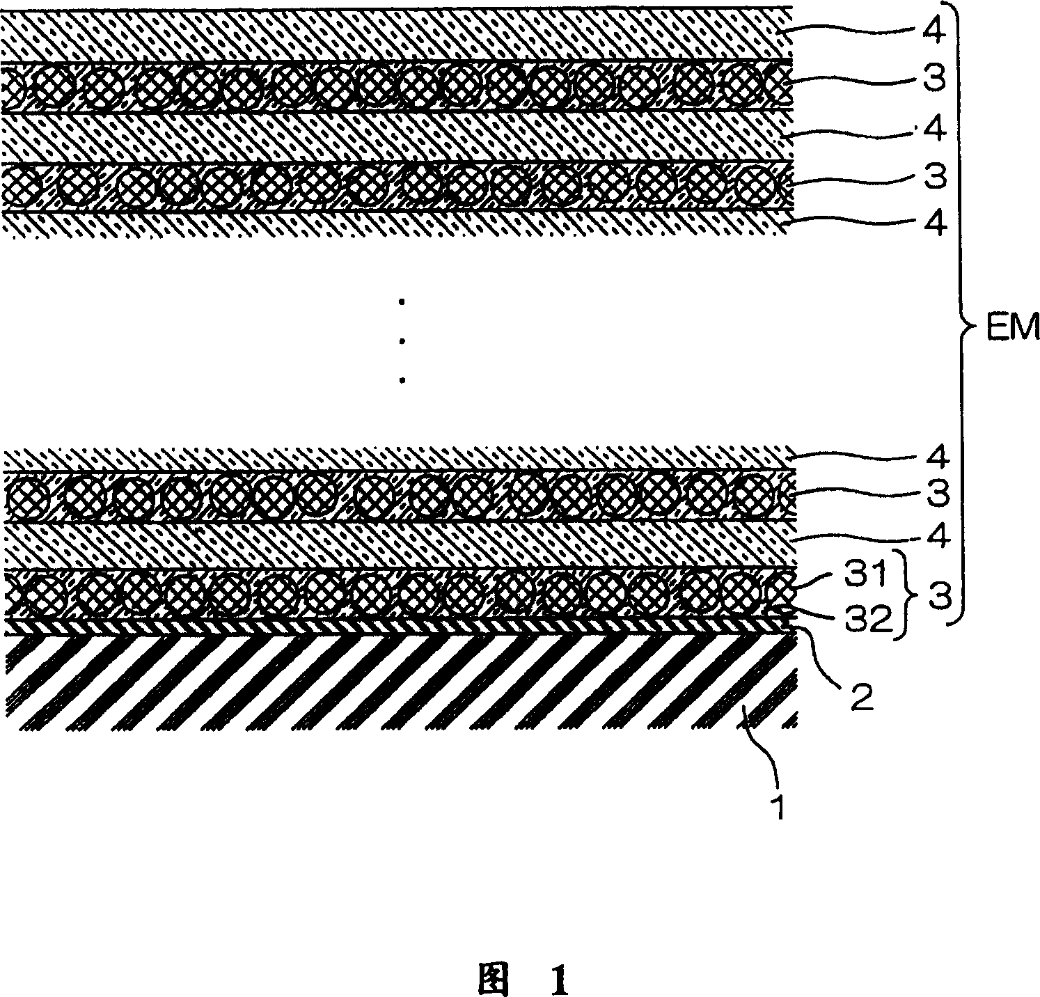
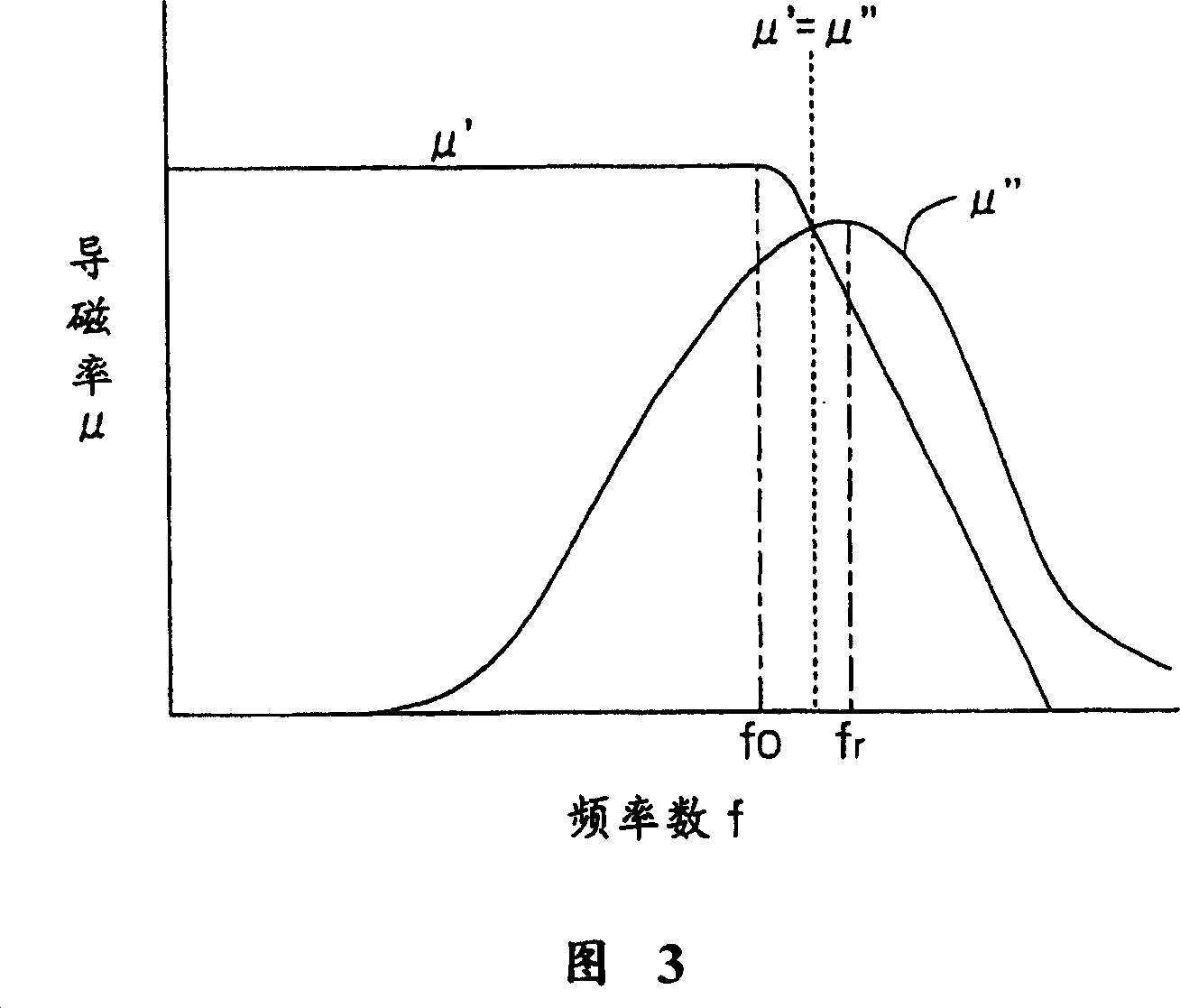

Image

  • Substrate for printed circuitboard distributing
  • Substrate for printed circuitboard distributing
  • Substrate for printed circuitboard distributing

Examples


Embodiment 1

[0208] 【Substrate】

[0209] One side surface of a 50 μm thick polyimide sheet was subjected to oxygen plasma treatment (output power 300W), and it was used as a base material for later use.

[0210] 【Formation of Adhesive Layer】

[0211] The components in the following Table 1 were mixed and stirred for 5 hours in an atmosphere with a relative humidity of 30%, whereby the hydrolysis reaction was carried out by the moisture in the atmosphere to generate a titanium sol solution.

[0212] Element

g

Isopropyl phthalate

Isopropanol

2-Ethylhexanoic acid

284

600

144

[0213] The surface treated with oxygen plasma was exposed, and the above-mentioned polyimide sheet masked on the opposite side was immersed in the above-mentioned titanium sol solution, and then lifted at a speed of 0.5 cm / min, thereby forming a titanium dioxide sol with a thickness of about 10 nm. Treat the membrane.

[0214] Then, the polyimide sheet was heated ...

Embodiment 2

[0224] In the same manner as in Example 1, except that the adhesive layer is formed by the following steps, on the surface of the polyimide sheet as the substrate through oxygen plasma treatment, a silicon dioxide titanium dioxide adhesive layer is laminated with 12 The electromagnetic wave absorbing layer of the layer-by-layer structure is made into a printed circuit board.

[0225] [Formation of Adhesive Layer]

[0226] The components in the following Table 2 were mixed, stirred for 5 hours in an atmosphere with a relative humidity of 30%, and hydrolyzed by the moisture in the atmosphere to generate a silicon-titanium sol solution.

[0227] Element

g

Isopropyl phthalate

tetrabutyl orthosilicate

Isopropanol

2-Ethylhexanoic acid

100

86

600

144

[0228] The surface treated with oxygen plasma is exposed, and the above-mentioned polyimide sheet masked on the opposite side is immersed in the above-mentioned silicon-ti...

Embodiment 3

[0231] Using a glass epoxy resin substrate with a thickness of 500 μm as the base material, except that the oxygen plasma treatment on its surface is omitted, the others are the same as in Example 1. On one side surface of the glass epoxy resin substrate, through a titanium dioxide adhesive layer, Electromagnetic wave absorbing layers having a laminated structure of 12 layers were laminated, thereby producing a printed circuit board.


PUM


Abstract

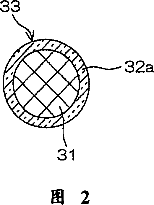
A board for printed wiring is provided on a surface of a substrate (1) with the intervention of an adhesive layer 2 of a metal oxide, the electromagnetic wave absorbing laminate (EM) comprising: (a) a magnetic layer 3 comprising a plurality of magnetic particles 31 having an average particle diameter of 1 to 150 nm and isolated from each other by an electrically insulative material 32; and (b) an electrically insulative layer 4, being alternately stacked in a multi-layer structure, the board for printed wiring has a reduced thickness and an improved electromagnetic wave absorbing characteristic in a high frequency band of not lower than gigahertz, as compared with a conventional one which has an electromagnetic wave absorbing layer of a composite material including fine magnetic particles simply dispersed in a resin binder.

Description

technical field [0001] The present invention relates to a new substrate for printed circuit wiring, which has a function of reducing unnecessary noise radiation from devices using high frequencies above gigahertz, such as mobile phones and laptop computers. Background technique [0002] In recent years, in order to reduce the emission of unwanted radiated noise from devices that use high frequencies above gigahertz, such as mobile phones and laptop computers, methods that utilize the magnetic loss of magnetic materials have attracted attention. [0003] The mechanism of electromagnetic wave absorption (which does not require attenuation of radiation noise) using the magnetic loss of a magnetic body is as follows: Although it varies with factors such as the positional relationship between the noise source and the magnetic body, by bringing the magnetic body very close to the noise transmission path, the Can suppress the generation of high-frequency current. [0004] In addit...

Claims


Application Information

Patent Timeline
Patent Type & Authority Patents(China)
IPC IPC(8): H05K9/00H05K1/02
CPCY10T428/24917H05K1/0233
Inventor 稻泽信二高田博史细江晃久新田耕司
Owner SUMITOMO ELECTRIC IND LTD
Learn More