Semiconductor memory

A memory and semiconductor technology, applied in the field of dynamic RAM, can solve problems such as low data transmission rate, high chip cost, and small storage capacity

Inactive Publication Date: 2006-05-31
SOCIONEXT INC
View PDF0 Cites 0 Cited by
  • Summary
  • Abstract
  • Description
  • Claims
  • Application Information

AI Technical Summary

Problems solved by technology

However, since the elements constituting each memory cell of SRAM are larger compared to DRAM, SRAM has the disadvantage of small storage capacity compared to DRAM
[0005] Since the memory controller of DRAM must also control the refresh operation, conventional DRAM has the disadvantage of complex control compared with SRAM
Conventional DRAM also suffers from a lower data transfer rate compared to SRAM since the read and write operations of DRAM cannot be performed during the refresh operation
[0006] On the other hand, due to the large size of the storage unit of SRAM, in addition to the above-mentioned difficulty in providing large capacity, SRAM also has the disadvantage of very high chip cost compared with DRAM

Method used


Image

  • Semiconductor memory
  • Semiconductor memory
  • Semiconductor memory

Examples


Embodiment Construction

[0033] Embodiments of the present invention are described below with reference to the drawings.

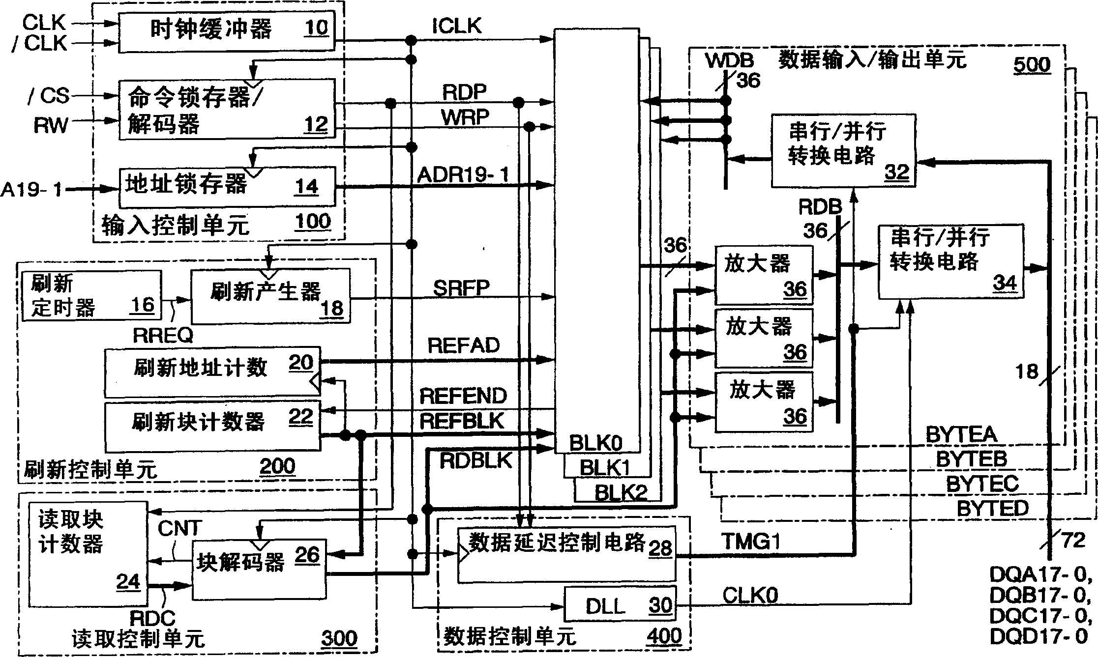
[0034] see figure 1 , which shows a first embodiment of a semiconductor memory according to the present invention. In this figure, each signal line indicated by a thick line is composed of a plurality of signal lines. Signals represented by a prefix with " / " represent negative logic.

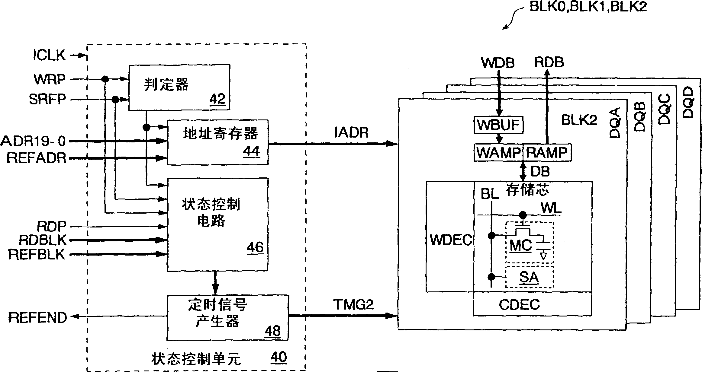
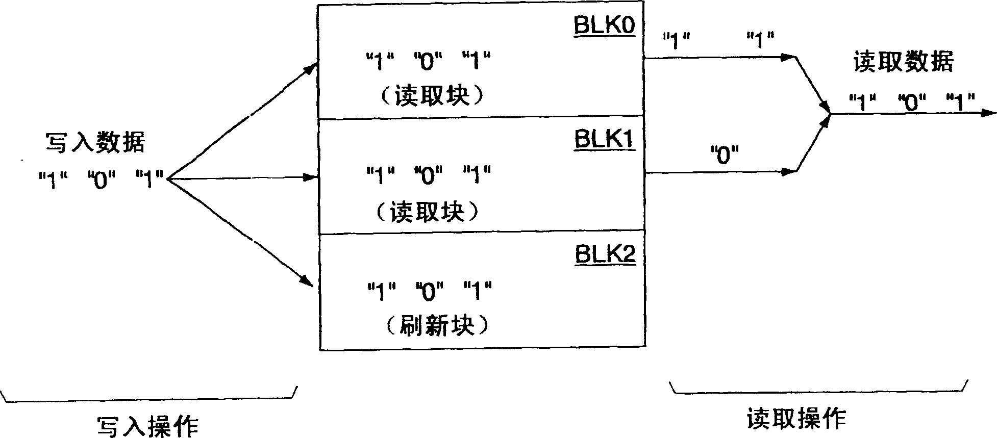
[0035] The semiconductor memory is formed as a clock-synchronized double data rate (DDR) pseudo-SRAM on a silicon substrate by using a CMOS process. DDR is an interface for inputting / outputting data in synchronization with rising and falling edges of a clock signal. The pseudo SRAM has an input control unit 100 , a refresh control unit 200 , a read control unit 300 , memory blocks BLK ( BLK0 - 2 ), a data control unit 400 and a data input / output unit 500 .

[0036] The pseudo SRAM also has input terminals for externally receiving clock signals CLK and / CLK, chip select signal / CS, read / write sig...


PUM


Abstract

A plurality of memory blocks are assigned the same address space to write the same data therein, and can be operated independently of each other. In response to a refresh command, one memory block is selected as a refresh block performing a refresh operation, and in response to a read command, another memory block is selected as a read block performing a read operation. Then, a plurality of memory blocks perform read operations at different timings so that the read operations overlap each other. Therefore, the semiconductor memory can receive a read command at a time interval shorter than the execution time of a single read operation. As a result, an externally supplied read command can be responded to at a high speed, and a data transfer rate during a read operation can be increased.

Description

technical field [0001] The present invention relates to a dynamic RAM that requires periodic refresh operations of memory cells. More particularly, the present invention relates to a technique for automatically performing a refresh operation internally without any refresh command from the outside. Background technique [0002] Dynamic RAMs (hereinafter referred to as DRAMs) are suitable for high integration because their memory cells can be formed smaller. However, DRAM requires a refresh operation for maintaining data stored in memory cells. This refresh operation must be performed periodically for all memory cells. When a flush command occurs, the flush operation must take priority over read or write operations. [0003] For example, in a system mounted with a DRAM, when a refresh command from a refresh timer of the memory controller occurs, a memory controller for controlling the DRAM supplies the refresh command to the DRAM before a read or write command. [0004] On...

Claims


Application Information

Patent Timeline
Patent Type & Authority Patents(China)
IPC IPC(8): H01L27/108G11C11/401G11C11/402G11C11/403G11C11/406G11C11/407G11C11/408
CPCG11C11/406G11C11/4087G11C11/402
Inventor 柳下良昌内田敏也阪東能英小林広之山口秀策奥田正樹
Owner SOCIONEXT INC
Why Eureka
Try Eureka