Ultraviolet-visible microobjective optical system for wafer AOI detection

A technology of microscope objective lens and optical system, applied in the field of ultraviolet-visible microscope objective lens optical system and optical system, can solve the problems of limited detection efficiency, small field of view on the object side, image quality influence, etc., to achieve high-resolution characteristics, The effect of reducing the amount of introduction

Active Publication Date: 2022-08-05
苏州瑞霏光电科技有限公司
View PDF19 Cites 1 Cited by
  • Summary
  • Abstract
  • Description
  • Claims
  • Application Information

AI Technical Summary

Problems solved by technology

[0006] According to the description of the invention patent, in order to reduce the number of lenses and improve the imaging quality, all residual aberrations are compensated and eliminated to the maximum extent through the aberration compensation relationship between the microscope objective lens and the tube lens, and the infinite conjugate microscope system Compared with the general design method of independent optimization of infinity point objects by the medium microscope objective lens and the tube lens, the image quality will be affected to a certain extent when the microscope objective lens is used alone
[0007] According to the description of the invention patent embodiment, the radius of the object-side field of view of the microscope objective lens is 0.2mm, that is, the object-side field of view is 0.4mm, and the object-side field of view is small, which limits the detection efficiency

Method used


Image

  • Ultraviolet-visible microobjective optical system for wafer AOI detection
  • Ultraviolet-visible microobjective optical system for wafer AOI detection
  • Ultraviolet-visible microobjective optical system for wafer AOI detection

Examples


Embodiment

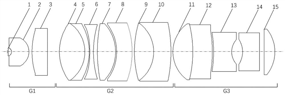
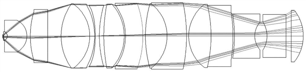
[0035] Example: A UV-Vis microscope objective optical system for wafer AOI inspection, such as figure 1 As shown, the object side is defined as the left side, and the image side is defined as the right side. Since the optical path is reversible, according to the reverse optical path design, the optical system of the microscope objective lens is along its optical axis direction from the object side to the image side, including the positive diopter in turn. The first lens group G1 (front group), the second lens group G2 (middle group) with positive diopter, and the third lens group G3 (rear group) with negative diopter, wherein:

[0036] The first lens group sequentially includes along its optical axis from the object side to the image side: a first lens 1 with positive refractive power, a second lens 2 with positive refractive power, and a third lens 3 with positive refractive power;

[0037]The second lens group sequentially includes along its optical axis from the object side...


PUM

PropertyMeasurementUnit
lengthaaaaaaaaaa
optical path lengthaaaaaaaaaa

Abstract

The invention discloses an ultraviolet-visible microobjective optical system for wafer AOI (automatic optical inspection), which sequentially comprises a first lens group, a second lens group and a third lens group from an object space to an image space along the optical axis direction of the ultraviolet-visible microobjective optical system, the first lens group comprises a first lens with positive focal power, a second lens with positive focal power and a third lens with positive focal power; the second lens group comprises a fourth lens with positive focal power, a fifth lens with positive focal power, a sixth lens with negative focal power, a seventh lens with positive focal power, an eighth lens with negative focal power, a ninth lens with positive focal power and a tenth lens with negative focal power; the third lens group includes an eleventh lens having a positive refractive power, a twelfth lens having a positive refractive power, a thirteenth lens having a negative refractive power, a fourteenth lens having a negative refractive power, and a fifteenth lens having a positive refractive power. The invention has the characteristics of large field of view and large numerical aperture.

Description

technical field [0001] The invention belongs to the technical field of optical instruments, and relates to an optical system, in particular to an ultraviolet-visible microscope objective optical system used for wafer AOI detection. Background technique [0002] The reduction in critical line width (CD) of lithographic patterns means less margin for various errors in chip fabrication packaging. Restricted by physical conditions, the lithography process cannot be completely accurate, and various processing procedures of the wafer may introduce a wide variety of complex defects, which will cause the output chips to become defective or even completely scrapped. The infinite conjugate microscopy imaging system includes a microscope objective lens and a tube lens, and the magnified wafer surface defect information is imaged on a CCD or CMOS. As an important part of the wafer AOI inspection equipment, its performance directly determines the wafer defect. Detection resolution and s...

Claims


Application Information

Patent Timeline
Patent Type & Authority Applications(China)
IPC IPC(8): G02B21/02G02B13/00G02B13/06G02B13/18
CPCG02B21/02G02B13/0045G02B13/006G02B13/06G02B13/18Y02P70/50
Inventor 解树平顾伟中
Owner 苏州瑞霏光电科技有限公司
Why Eureka
Try Eureka