Cap-layer-free InP HEMT ohmic contact structure, terahertz detector and manufacturing method thereof
A technology of ohmic contact and fabrication method, applied in semiconductor devices, electric solid state devices, semiconductor/solid state device parts and other directions, can solve the problems of gate leakage, affecting the effective work function of the gate metal, reducing the sensitivity of the detector, etc., to achieve simplification The effect of preparation process, improved transport characteristics, and improved sensitivity
- Summary
- Abstract
- Description
- Claims
- Application Information
AI Technical Summary
Problems solved by technology
Method used
Image


Examples
Embodiment 1
[0057] A fabrication method of a terahertz detector based on a capless InP HEMT, comprising:
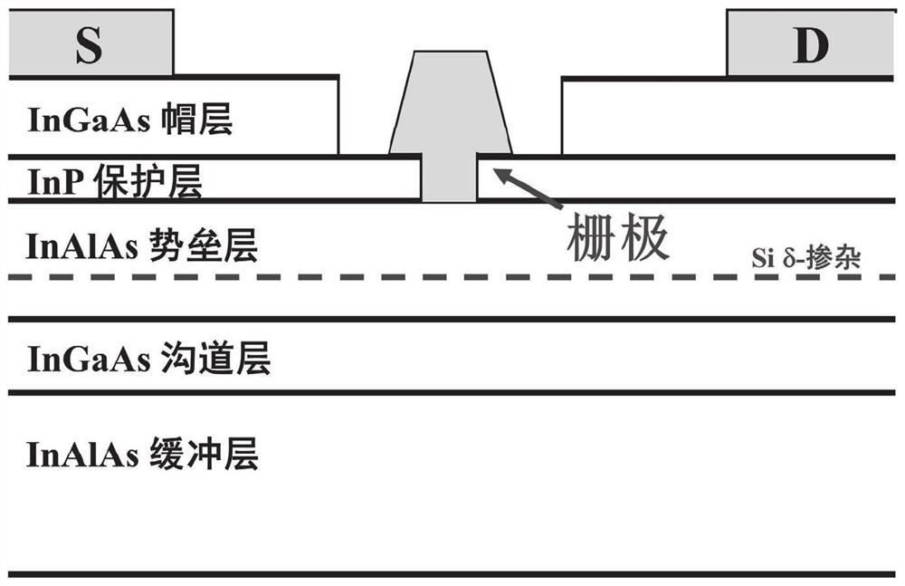
[0058] On the InP substrate, the InGaAs / InAs / InGaAs=2nm / 5nm / 3nm composite channel layer and the 11nm InAlAs barrier layer, which are stacked in sequence, are fabricated. The composite channel layer and the InAlAs barrier layer form a heterojunction, so A two-dimensional electron gas is formed between the composite channel layer and the InAlAs barrier layer;
[0059] Mesa isolation is formed by dry etching the InAlAs barrier layer by ICP, and Ni / Ge / Au ohmic contact metal is fabricated by electron beam evaporation, etc. 2 Atmosphere, annealed at 200 °C for 20 seconds, and annealed at 340 °C for 80 seconds, the specific contact resistivity of the uncapped InP HEMT reached 1.80 × 10 -2 Ω·cm 2 ;
[0060] Pt(7nm) / Ti(30nm) / Pt(20nm) / Au(180nm) gate metal and antenna were fabricated by electron beam evaporation; Ni(30nm) / Au(300nm) thickened lead electrodes were fabricated by electron beam e...
Embodiment 2
[0062] A fabrication method of a terahertz detector based on a capless InP HEMT, comprising:
[0063] On the InP substrate, the InGaAs / InAs / InGaAs=2nm / 5nm / 3nm composite channel layer and the 11nm InAlAs barrier layer, which are stacked in sequence, are fabricated. The composite channel layer and the InAlAs barrier layer form a heterojunction, so A two-dimensional electron gas is formed between the composite channel layer and the InAlAs barrier layer;
[0064] Mesa isolation is formed by dry etching the InAlAs barrier layer by ICP, and Ni / Ge / Au ohmic contact metal is fabricated by electron beam evaporation, etc. 2 Atmosphere, annealed at 200 °C for 20 seconds, and annealed at 380 °C for 80 seconds, the specific contact resistivity of the uncapped InP HEMT reached 2.94 × 10 -3 Ω·cm 2 ;
[0065] Pt(7nm) / Ti(30nm) / Pt(20nm) / Au(180nm) gate metal and antenna were fabricated by electron beam evaporation; Ni(30nm) / Au(300nm) thickened lead electrodes were fabricated by electron beam e...
Embodiment 3
[0067] A fabrication method of a terahertz detector based on a capless InP HEMT, comprising:
[0068] On the InP substrate, the InGaAs / InAs / InGaAs=2nm / 5nm / 3nm composite channel layer and the 11nm InAlAs barrier layer, which are stacked in sequence, are fabricated. The composite channel layer and the InAlAs barrier layer form a heterojunction, so A two-dimensional electron gas is formed between the composite channel layer and the InAlAs barrier layer;
[0069] Mesa isolation is formed by dry etching the InAlAs barrier layer by ICP, and Ni / Ge / Au ohmic contact metal is fabricated by electron beam evaporation, etc. 2 Atmosphere, annealed at 200 °C for 20 seconds, and annealed at 370 °C for 50 seconds, the specific contact resistivity of the uncapped InP HEMT reached 6.22×10 -4 Ω·cm 2 ;
[0070] Pt(7nm) / Ti(30nm) / Pt(20nm) / Au(180nm) gate metal and antenna were fabricated by electron beam evaporation; Ni(30nm) / Au(300nm) thickened lead electrodes were fabricated by electron beam eva...
PUM
| Property | Measurement | Unit |
|---|---|---|
| thickness | aaaaa | aaaaa |
| thickness | aaaaa | aaaaa |
| thickness | aaaaa | aaaaa |
Abstract
Description
Claims
Application Information
 - R&D
- Intellectual Property
- Life Sciences
- Materials
- Tech Scout
- Unparalleled Data Quality
- Higher Quality Content
- 60% Fewer Hallucinations
Browse by: Latest US Patents, China's latest patents, Technical Efficacy Thesaurus, Application Domain, Technology Topic, Popular Technical Reports.
© 2025 PatSnap. All rights reserved.Legal|Privacy policy|Modern Slavery Act Transparency Statement|Sitemap|About US| Contact US: help@patsnap.com