Super junction device manufacturing method, super junction device, chip and circuit

A manufacturing method and super-junction technology, which is applied in semiconductor/solid-state device manufacturing, circuits, semiconductor devices, etc., can solve the problems that the uniformity of trench etching depth is difficult to control, and epitaxial filling is easy to form voids, etc., so as to improve epitaxial filling voids , Reduce the difficulty of trench etching, and reduce the effect of trench aspect ratio

Inactive Publication Date: 2022-07-29
BEIJING CHIP IDENTIFICATION TECH CO LTD +1
View PDF10 Cites 1 Cited by
  • Summary
  • Abstract
  • Description
  • Claims
  • Application Information

AI Technical Summary

Problems solved by technology

[0005] Aiming at the technical problems in the prior art that the uniformity of trench etching depth is difficult to control and voids are easily formed during epitaxial filling, the present invention provides a method for manufacturing a super junction device, a super junction device, a chip and A circuit, the method can reduce the difficulty of trench etching, reduce the depth of trench etching, improve the uniformity of trench etching depth, reduce the aspect ratio of trenches, and improve epitaxial filling of voids

Method used


Image

  • Super junction device manufacturing method, super junction device, chip and circuit
  • Super junction device manufacturing method, super junction device, chip and circuit
  • Super junction device manufacturing method, super junction device, chip and circuit

Examples


Embodiment Construction

[0029] The specific implementations of the embodiments of the present invention will be described in detail below with reference to the accompanying drawings. It should be understood that the specific implementation manners described herein are only used to illustrate and explain the embodiments of the present invention, and are not used to limit the embodiments of the present invention.

[0030] It should be noted that the embodiments of the present invention and the features of the embodiments may be combined with each other under the condition of no conflict.

[0031] In the present invention, unless otherwise stated, the directional words used such as "upper, lower, top, bottom" are usually for the direction shown in the drawings or for the vertical, vertical or gravity direction The words used to describe the mutual positional relationship of the components mentioned above.

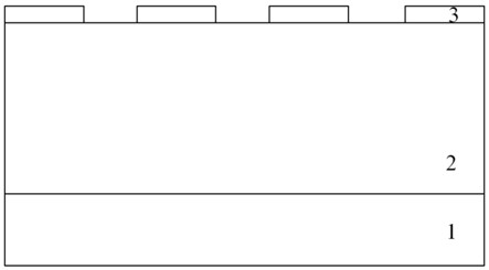
[0032] The present invention will be described in detail below with reference to the accompanyin...


PUM


Abstract

The invention provides a manufacturing method of a super junction device, the super junction device, a chip and a circuit, and belongs to the technical field of semiconductors, and the manufacturing method comprises the steps: providing a substrate with an epitaxial layer; defining an etching region on the upper surface of the epitaxial layer; forming an etching groove with a first depth in the epitaxial layer by using an etching process according to the etching region; performing ion implantation on the bottom of the etching groove to form a doped region, wherein the doped region has a second conduction type, and the sum of the second depth and the first depth of the doped region is equal to the target depth; epitaxial filling is carried out on the etching groove to form a filling area, and a super junction is formed by a longitudinal doping area formed by the filling area and the doping area and an adjacent epitaxial layer area; a gate and a body region are formed, the body region is located at the top of the longitudinal doping region, and the gate is located on the upper surface of the epitaxial layer and covers part of the body region. Through the method provided by the invention, the uniformity of the etching depth of the groove is improved, the depth-to-width ratio of the groove is reduced, and epitaxial filling holes are improved.

Description

technical field [0001] The present invention relates to the technical field of semiconductors, and in particular, to a method for manufacturing a super junction device, a super junction device, a chip and a circuit. Background technique [0002] Power semiconductor devices are widely used in power supplies or adapters for consumer electronic products such as mobile phones, computers, lighting, and LCD TVs. Traditional power semiconductor devices have a contradiction between breakdown voltage and on-resistance, that is, the on-resistance of power semiconductor devices has a limit due to the limitation of breakdown voltage. In order to break this limitation, super junction devices appear. [0003] The super junction consists of alternately arranged P-type semiconductor thin layers (referred to as P-pillars) and N-type semiconductor thin layers (referred to as N-pillars). This structure enables charge compensation by depleting the P and N pillars at lower voltages in the off-s...

Claims


Application Information

Patent Timeline
Patent Type & Authority Applications(China)
IPC IPC(8): H01L21/8234H01L27/088H01L29/06
CPCH01L29/0634H01L21/823493H01L27/088
Inventor 赵东艳王于波陈燕宁田俊付振张泉肖超尹强
Owner BEIJING CHIP IDENTIFICATION TECH CO LTD
Why Eureka
Try Eureka