Flip LED chip and production process thereof

A technology of LED chip and production process, which is applied in the direction of semiconductor devices, electrical components, circuits, etc., can solve the problems of poor thermal conductivity of flip-chip LED chips, falling off of flip-chip LED chips, and small contact area, so as to achieve good light extraction efficiency and prevent Detachment of virtual soldering and good interface morphology

Pending Publication Date: 2022-07-22
飞尼科斯(苏州)电子有限公司
View PDF2 Cites 0 Cited by
  • Summary
  • Abstract
  • Description
  • Claims
  • Application Information

AI Technical Summary

Problems solved by technology

[0005] When the flip-chip LED chip in the prior art is soldered, its contact area is small, resulting in poor thermal conductivity of the flip-chip LED chip, and prone to virtual soldering, which makes the flip-chip LED chip easy to fall off from the substrate

Method used


Image

  • Flip LED chip and production process thereof
  • Flip LED chip and production process thereof
  • Flip LED chip and production process thereof

Examples


Embodiment Construction

[0034] In order to make those skilled in the art better understand the technical solutions of the present invention, the present invention will be further described in detail below with reference to the accompanying drawings.

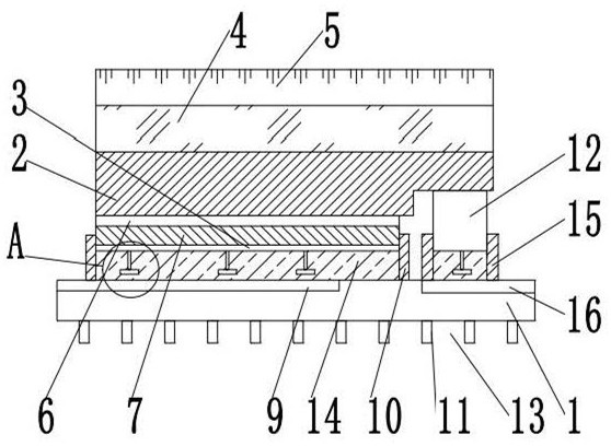
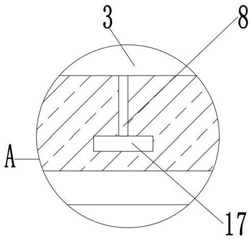
[0035] like Figure 1-3 As shown, a flip-chip LED chip provided by an embodiment of the present invention includes a substrate 1, an n-pole conductive plate 9 and a p-pole conductive plate 16 are embedded in the top of the substrate 1, and a positioning frame is welded on the top of the n-pole conductive plate 9 One 10, the top of the p-pole conductive plate 16 is welded with a positioning frame 2 15, the top of the substrate 1 is provided with a p-type gallium nitride layer 2, and the bottom outer wall of the p-type gallium nitride layer 2 is provided with an n-type gallium nitride layer 7 The bottom outer wall of the n-type gallium nitride layer 7 is provided with an n-electrode 3 , the n-type gallium nitride layer 7 is located inside the positioning ...


PUM

PropertyMeasurementUnit
thicknessaaaaaaaaaa
thicknessaaaaaaaaaa
thicknessaaaaaaaaaa

Abstract

The flip LED chip comprises a substrate, an n-pole conductive plate and a p-pole conductive plate are embedded in the top of the substrate, a first positioning frame is welded to the top of the n-pole conductive plate, a second positioning frame is welded to the top of the p-pole conductive plate, a p-type gallium nitride layer is arranged on the top of the substrate, an n-type gallium nitride layer is arranged on the outer wall of the bottom of the p-type gallium nitride layer, and the n-type gallium nitride layer is arranged on the outer wall of the bottom of the p-type gallium nitride layer. An n electrode is arranged on the outer wall of the bottom of the n-type gallium nitride layer, the n-type gallium nitride layer is located in the first positioning frame, and welding materials are arranged in the first positioning frame and the second positioning frame. According to the flip LED chip, the welding materials are added into the positioning frame I and the positioning frame II, and the welding materials are welded with the n-pole conductive plate and the p-pole conductive plate after being melted, so that the electrode contact surface of the flip LED chip is increased, and the heat conduction effect of the flip LED chip is improved.

Description

technical field [0001] The invention relates to the technical field of LED chips, in particular to a flip-chip LED chip and a production process thereof. Background technique [0002] A light-emitting diode is a semiconductor solid-state light-emitting device, which is made using the electroluminescence principle of a semiconductor PN junction. LED devices have good optoelectronic properties such as low turn-on voltage, small size, fast response, good stability, long life, and no pollution. Therefore, they are widely used in outdoor and indoor lighting, backlight, display, traffic indication and other fields. Generally speaking, LED chips are divided into three types: horizontal structure (front-mounted chip), vertical structure (vertical structure chip) and flip-chip structure (flip-chip). Among them, the P and N electrode layers in the flip-chip LED chip are located in On the same side of the light-emitting region, the light emitted by the active layer in the LED chip mai...

Claims


Application Information

Patent Timeline
Patent Type & Authority Applications(China)
IPC IPC(8): H01L33/62H01L33/64H01L33/36H01L33/40
CPCH01L33/62H01L33/647H01L33/36H01L33/40H01L2933/0066
Inventor 薛谆薛龄
Owner 飞尼科斯(苏州)电子有限公司
Why Eureka
Try Eureka