Plasma processing device and plasma processing method

A plasma and processing device technology, applied to circuits, discharge tubes, electrical components, etc., can solve problems such as unfavorable stable operation and damage of plasma processing devices, and achieve the effects of improving stability, reducing phenomena, and ensuring uniformity

Pending Publication Date: 2022-07-01
ADVANCED MICRO FAB EQUIP INC CHINA
View PDF0 Cites 0 Cited by
  • Summary
  • Abstract
  • Description
  • Claims
  • Application Information

AI Technical Summary

Problems solved by technology

[0005] With the development of the process, part of the etching process will produce thicker deposits on the surface of the parts. In the cleaning step, in order to ensure the cleaning effect of the deposits, it is necessary to apply a relatively high-power radio frequency signal to the electrostatic chuck. , since the electrostatic chuck is exposed to the cleaning plasma, some areas may be damaged by the bombardment of the cleaning plasma, which is not conducive to the stable operation of the plasma processing device. Therefore, it is necessary to provide a plasma that can work stably in the cleaning step processing device

Method used


Image

  • Plasma processing device and plasma processing method
  • Plasma processing device and plasma processing method
  • Plasma processing device and plasma processing method

Examples


Embodiment Construction

[0032] The technical solutions in the embodiments of the present invention will be clearly and completely described below with reference to the accompanying drawings in the embodiments of the present invention. Obviously, the described embodiments are only a part of the embodiments of the present invention, but not all of the embodiments. Based on the embodiments of the present invention, all other embodiments obtained by those of ordinary skill in the art without creative efforts shall fall within the protection scope of the present invention.

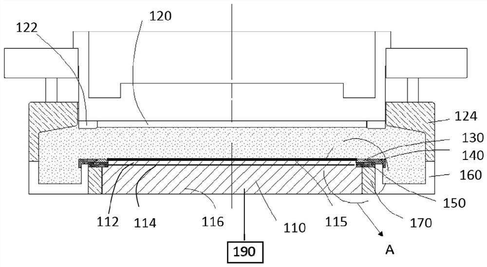
[0033] figure 1 A plasma processing apparatus is shown, including a reaction chamber, the reaction chamber includes an upper electrode assembly and a lower electrode assembly arranged oppositely, and the upper electrode assembly includes a gas shower head 120 and an upper ground disposed around the gas shower head. Ring 122, the gas shower head is used for delivering process gas or cleaning gas into the reaction chamber, and at the sa...


PUM

PropertyMeasurementUnit
widthaaaaaaaaaa

Abstract

The invention discloses a plasma processing device and method, and the device comprises a reaction chamber, and the reaction chamber comprises a gas inlet device which is used for conveying clean gas to the reaction chamber; the radio frequency power supply is used for dissociating the clean gas into clean plasma; a cleaning wafer having a first diameter; and the electrostatic chuck is used for bearing the cleaning wafer and has a second diameter, and the difference value between the first diameter and the second diameter is smaller than or equal to + / -0.5 mm. In the cleaning step, the cleaning wafer with the size close to that of the electrostatic chuck 110 is adopted to cover the surface of the electrostatic chuck, the damage degree of cleaning plasma to the upper surface of the electrostatic chuck can be effectively reduced, meanwhile, the cleaning wafer cannot shield the second upper surface 134 of the focusing ring and a gap between the focusing ring and the electrostatic chuck, and the cleaning efficiency is improved. Sediments on the second upper surface of the focusing ring and in the gap can be effectively removed by the cleaning plasma.

Description

technical field [0001] The present invention relates to the field of semiconductor equipment, in particular to the technical field of plasma cleaning. Background technique [0002] In the fabrication of semiconductor devices, plasma etching is a key process for processing wafers into designed patterns. [0003] In a typical plasma etch process, process gases such as CF 4 , O 2 etc.) in the reaction chamber to form plasma under the action of radio frequency (RadioFrequency, RF) excitation. These plasmas physically bombard and chemically react with the wafer surface to etch wafers with specific structures. [0004] After the wafer is etched, the wafer is taken out by moving the manipulator. In order to ensure the uniformity of wafer processing in different batches, after the wafer is moved out of the reaction chamber, the reaction chamber needs to be cleaned by plasma, and the reaction chamber needs to be cleaned by plasma. Enter the cleaning gas, apply radio frequency to ...

Claims


Application Information

Patent Timeline
Patent Type & Authority Applications(China)
IPC IPC(8): H01J37/32
CPCH01J37/32862H01J37/32477
Inventor 周艳倪图强
Owner ADVANCED MICRO FAB EQUIP INC CHINA
Why Eureka
Try Eureka