


Quick Research
Generate reliable direction feasibility study reports for your R&D in just a few steps.

Technical Q&A
Discover and master advanced knowledge NOW. Basics, ideas, possibilities, all at once.

Find Solutions
As an expert in R&D theories, this can generate solutions to your technical problems instantly.

Evaluate Feasibility
Analyze your overall solution with one click, know your potential R&D risks in advance.

Monitor Landscape
Get weekly tech updates, stay abreast of the latest tech innovations and key insights.
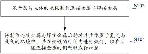
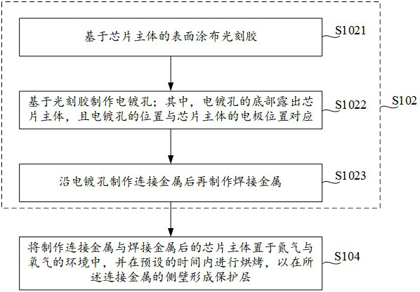
Chip manufacturing method, chip connecting method and chip
A production method and connection method technology, which is applied in semiconductor/solid-state device manufacturing, semiconductor/solid-state device parts, semiconductor devices, etc., can solve problems such as solder diffusion and chip failure, and achieve stable performance
- Summary
- Abstract
- Description
- Claims
- Application Information
AI Technical Summary
Problems solved by technology
Method used
Image

Examples
Embodiment Construction
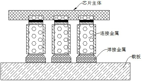
[0045] After making the chip theme, a layer of photoresist can be coated on the surface of the chip body, and the structure after coating the photoresist is as follows Figure 4 shown. Figure 4 In , the chip body includes electrodes, and the chip body also includes a metal layer, wherein the metal layer may be multi-layered, such as Figure 4 Among them, the metal layer can be two layers, and the metal layer can be used to realize different functions, for example, to realize Schottky contact, etc., which is not limited here. In the manufacturing process of the present application, the metal layer is actually deposited first, then photoresist is coated on the surface of the metal layer, and the photoresist is grooved to form plating holes.
[0046] It should also be noted that in the chip manufacturing process, multiple chips are actually manufactured at the same time, such as Figure 4 , shows the production of two chips, one chip is on the left side of the dotted line A, a...
PUM
 Abstract
Description
Claims
Application Information
 - R&D Engineer
- R&D Manager
- IP Professional
- Industry Leading Data Capabilities
- Powerful AI technology
- Patent DNA Extraction
Browse by: Latest US Patents, China's latest patents, Technical Efficacy Thesaurus, Application Domain, Technology Topic, Popular Technical Reports.
© 2024 PatSnap. All rights reserved.Legal|Privacy policy|Modern Slavery Act Transparency Statement|Sitemap|About US| Contact US: help@patsnap.com