Ceramic-based PCB (Printed Circuit Board) structure with embedded component and preparation process of ceramic-based PCB structure

A technology of ceramic substrate and PCB board, which is applied in the direction of printed circuits, electrical components, and circuit substrate materials connected with non-printed electrical components, which can solve the problems of difficult to meet the requirements of heat dissipation and not considering the overall heat dissipation of the PCB board. , to increase the integration effect, facilitate the development of miniaturization, and solve the needs of excessive number of components and heat dissipation

Pending Publication Date: 2022-06-07
CHENGYI ELECTRONICS JIAXING
View PDF0 Cites 0 Cited by
  • Summary
  • Abstract
  • Description
  • Claims
  • Application Information

AI Technical Summary

Problems solved by technology

[0003] At present, most of the commonly used heat dissipation methods are: 1. Through copper cladding on the inner layer of the PCB, the heat of the heating components is dispersed to the copper cladding layer to realize PCB heat dissipation. Difficult to meet heat dissipation requirements; 2. Paste heat dissipation aluminum sheets on the surface of the power tube. This heat dissipation method only achieves local heat dissipation, and does not take into account the overall heat dissipation of the PCB board.

Method used


Image

  • Ceramic-based PCB (Printed Circuit Board) structure with embedded component and preparation process of ceramic-based PCB structure

Examples


Embodiment Construction

[0031] In order to enable those skilled in the art to better understand the technical solutions of the present invention, the preferred embodiments of the present invention will be described below in conjunction with specific examples, but it should be understood that the accompanying drawings are for illustrative purposes only, and cannot be interpreted as an explanation of this patent. Restrictions; In order to better illustrate this embodiment, some parts in the drawings will be omitted, enlarged or reduced, and do not represent the size of the actual product; for those skilled in the art, some known structures and their descriptions in the drawings may Omissions are understandable. The positional relationship described in the drawings is for illustrative purposes only, and should not be construed as a limitation on this patent.

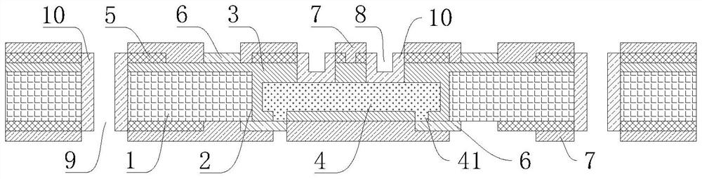
[0032] A ceramic-based PCB board structure with embedded components, including a ceramic substrate 1, a buried groove 2 is opened in the middle o...


PUM


Abstract

The invention discloses a ceramic-based PCB structure with an embedded component and a preparation process thereof, the ceramic-based PCB structure with the embedded component comprises a ceramic substrate, an embedded groove is formed in the middle of the ceramic substrate, photosensitive resin is laid in the embedded groove and on the upper surface of the ceramic substrate, and the component is embedded in the embedded groove; electroplated layers are respectively arranged on the upper surface of the photosensitive resin and the lower surface of the ceramic substrate; a circuit layer is arranged on the electroplated layer, and a solder mask layer is arranged on the outer surface of the electroplated layer. A metal substrate of a PCB in the prior art is replaced by the ceramic substrate, and the ceramic substrate has good thermal conductivity and insulativity, so that electronic components are not only assembled on the surface of the PCB of the ceramic substrate, but also can be embedded in the PCB of the ceramic substrate, and the requirements of too many components and heat dissipation can be met at the same time; meanwhile, the embedded groove is formed, and the components are installed in the embedded groove, so that the integration effect of the PCB bearing the components is improved, and miniaturization development of electronic products is facilitated.

Description

technical field [0001] The invention relates to the technical field of PCB boards, in particular to a ceramic-based PCB board structure with embedded components and a preparation process thereof. Background technique [0002] With the development of electronic design and manufacturing industry, Yu Laiyu of electronics and related industries pays attention to the development of electronic components in the direction of light, thin, short, small and high performance. There are more and more electronic components that need to be carried on a unit PCB board. At the same time, the accompanying heat is becoming more and more serious, so the heat dissipation capability directly affects the maximum working environment temperature and product life of the product as a whole. [0003] At present, most of the commonly used heat dissipation methods are: 1. Through copper cladding on the inner layer of the PCB, the heat of the heating components is dispersed to the copper cladding layer t...

Claims


Application Information

Patent Timeline
Patent Type & Authority Applications(China)
IPC IPC(8): H05K1/03H05K1/02H05K1/18H05K3/00H05K3/34
CPCH05K1/0306H05K1/0203H05K1/183H05K3/0029H05K3/0044H05K3/0094H05K3/3447
Inventor 张本贤李志雄舒志迁魏和平陈蓁邱锡曼
Owner CHENGYI ELECTRONICS JIAXING
Why Eureka
Try Eureka