Lateral light mode control high-power semiconductor device and preparation method thereof
A semiconductor, high-power technology, applied in the direction of semiconductor devices, electrical components, circuits, etc., can solve the problems of high beam quality, high brightness, high integration, etc., to achieve the effect of improving the brightness of the light, reducing the divergence angle, and increasing the thermal conductivity
- Summary
- Abstract
- Description
- Claims
- Application Information
AI Technical Summary
Problems solved by technology
Method used
Image
Examples
Embodiment 1
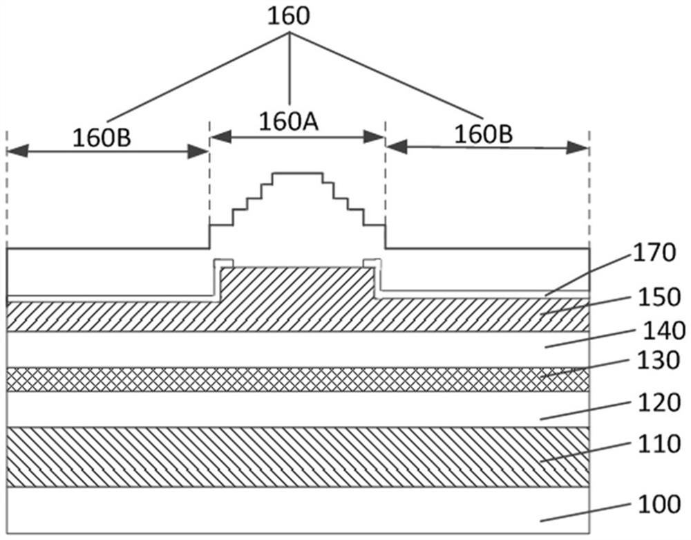
[0044] An embodiment of the present invention provides a side light mode control high-power semiconductor device, refer to figure 1 ,include:
[0045] Semiconductor substrate layer 100;
[0046] an active layer 130 located on the semiconductor substrate layer 100;
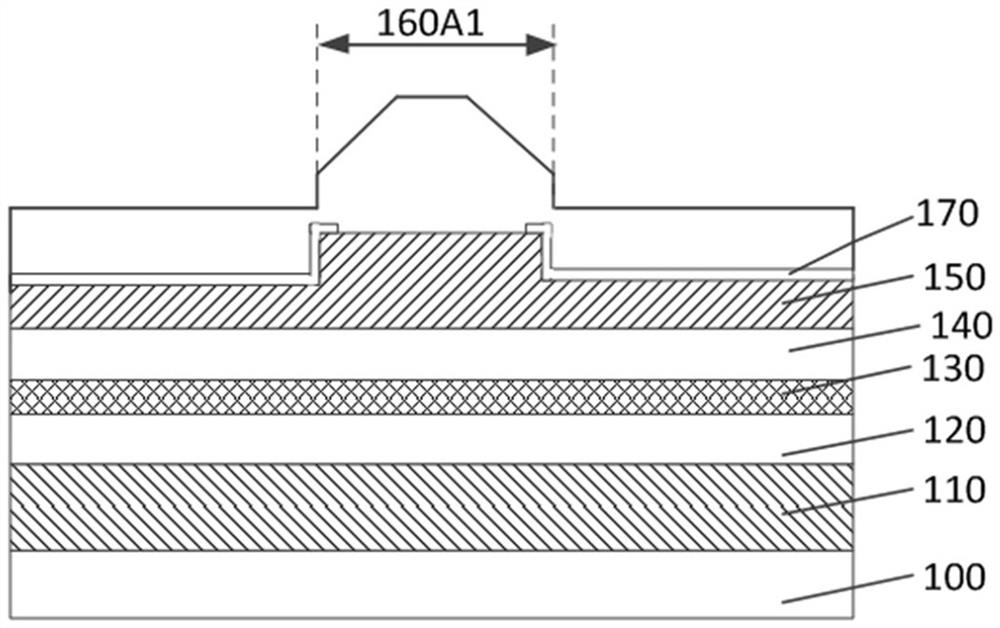
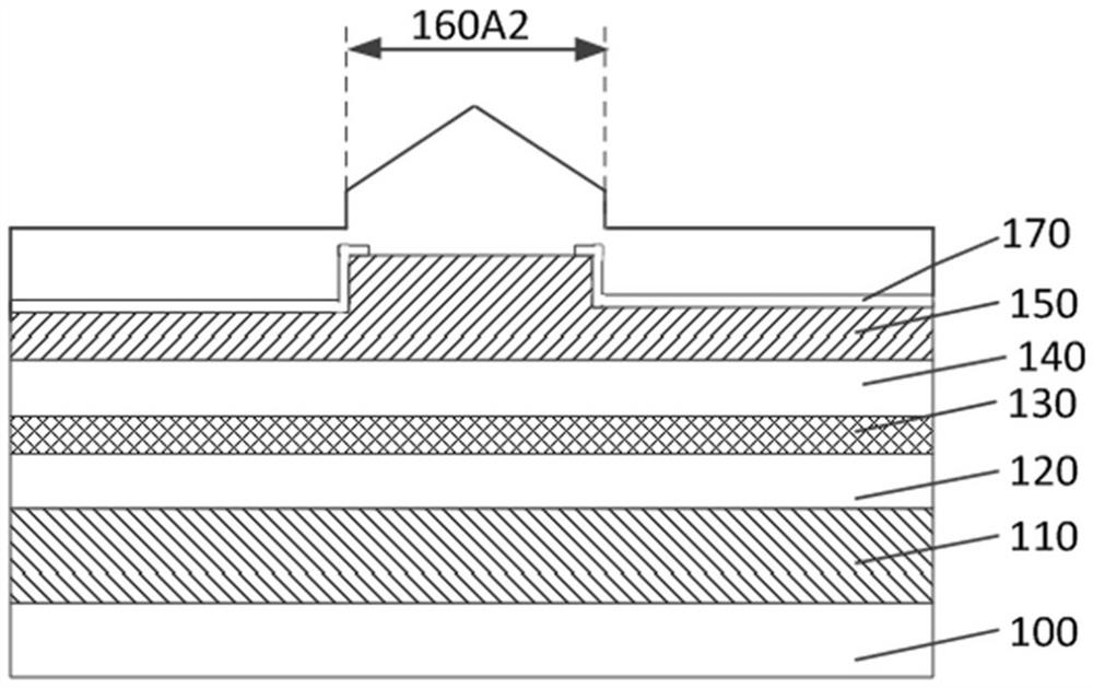
[0047] The front electrode layer 160 located on the side of the active layer 130 away from the semiconductor substrate layer 100, the front electrode layer 160 includes an electrode injection region 160A; From the central region of the electrode injection region 160A to the edge region of the electrode injection region 160A, the thickness of the electrode injection region 160A decreases gradually.
[0048] In this embodiment, the side-light mode control high-power semiconductor device is an edge-emitting semiconductor laser.
[0049] The material of the semiconductor substrate layer 100 includes silicon, gallium arsenide or aluminum gallium arsenide. In other embodiments, the material of the semiconductor subst...
Embodiment 2
[0075] The difference between this embodiment and embodiment 1 is: refer to Figure 6 , the lateral light mode control high-power semiconductor device further includes: a thermal compensation layer 210, the thermal compensation layer 210 is located on the side of the non-injection electrode region 160B facing the active layer 130 and is in contact with the non-injection electrode region 160B, the thermal compensation layer The thermal conductivity of the solder layer is less than that of the solder layer.
[0076] In this embodiment, since the thermal conductivity of the thermal compensation layer 210 is smaller than the thermal conductivity of the solder layer, the thermal conductivity of the thermal compensation layer 210 is smaller, reducing the impact of the semiconductor film directly below the thermal compensation layer 210 on non-injection. The degree of thermal conductivity of the electrode region 160B reduces the temperature gradient of the active layer 130 directly b...
Embodiment 3
[0090] The difference between this embodiment and embodiment 2 is: reference Figure 7 , the thermal compensation layer 210a includes a first compensation region M1 and a second compensation region M2 arranged in the direction of the slow axis, the distance from the first compensation region M1 to the electrode injection region 160A is smaller than that of the second compensation region M2 The distance to the electrode injection region 160A; the thickness of the second compensation region M2 is greater than the thickness of the first compensation region M1.
[0091] against Figure 7 The thermal compensation layer, the effect simulation picture is as follows Figure 8 ,and Figure 7 structure while comparing the figure 1 and Figure 6 The structure, by increasing the thickness of the second compensation region M2, the temperature of the active layer under the first compensation region M1 adjacent to the ridge region is further increased, the active layer under the first co...
PUM
| Property | Measurement | Unit |
|---|---|---|
| Thickness | aaaaa | aaaaa |
| Thickness | aaaaa | aaaaa |
| Thickness | aaaaa | aaaaa |
Abstract
Description
Claims
Application Information
 - R&D
- Intellectual Property
- Life Sciences
- Materials
- Tech Scout
- Unparalleled Data Quality
- Higher Quality Content
- 60% Fewer Hallucinations
Browse by: Latest US Patents, China's latest patents, Technical Efficacy Thesaurus, Application Domain, Technology Topic, Popular Technical Reports.
© 2025 PatSnap. All rights reserved.Legal|Privacy policy|Modern Slavery Act Transparency Statement|Sitemap|About US| Contact US: help@patsnap.com


