Rapid optimization method for half-space mapping of microstrip circuit in combination with Gaussian process

A microstrip circuit and Gaussian process technology, applied in CAD circuit design, special data processing applications, etc., can solve the problems of difficult optimal structure of neural network, high consumption of computer resources, and many initial training samples, and reduce the number of training samples. , the effect of less optimization parameters and faster convergence speed

Pending Publication Date: 2022-05-13
UNIV OF ELECTRONICS SCI & TECH OF CHINA
View PDF0 Cites 0 Cited by
  • Summary
  • Abstract
  • Description
  • Claims
  • Application Information

AI Technical Summary

Problems solved by technology

[0004] For the low efficiency and high consumption of computer resources in the design process of multi-structure parameters of microstrip circuits; in the traditional neural-space mapping optimization technology, it is difficult to determine the optimal structure of the neural network, the required initial training samples are large, and the directionality of optimization is not optimized. Judgment and other issues, the present invention provides a fast optimization method for microstrip circuit half-space mapping combined with Gaussian process

Method used


Image

  • Rapid optimization method for half-space mapping of microstrip circuit in combination with Gaussian process
  • Rapid optimization method for half-space mapping of microstrip circuit in combination with Gaussian process
  • Rapid optimization method for half-space mapping of microstrip circuit in combination with Gaussian process

Examples


Embodiment Construction

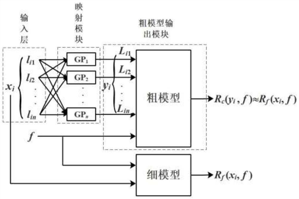
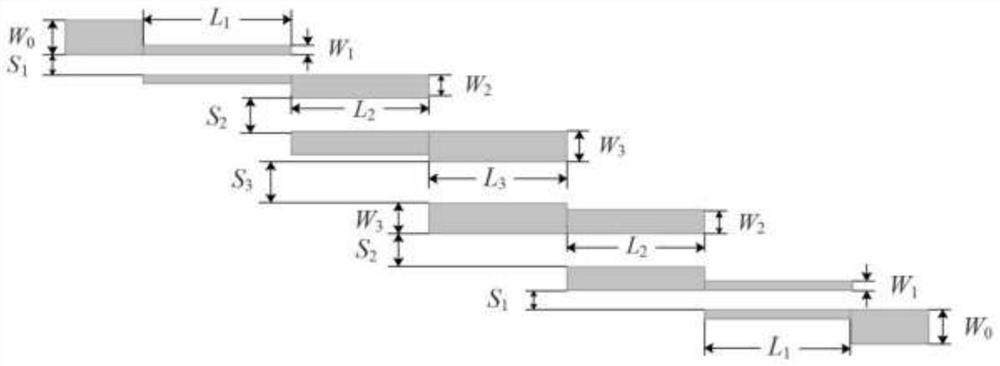
[0031] In order to show the technical scheme and beneficial effect of the present invention more clearly and clearly, now combine a image 3 The W-band microstrip parallel coupled filter design example shown is illustrated.

[0032] The dielectric substrate adopted by the filter of this embodiment has a relative permittivity of ε r =3.8 fused silica substrate with a thickness of 0.1 mm. The width of each microstrip line has been determined, respectively W 0 =0.211mm, W 1 = 0.1mm, W 2 = 0.16mm, W 3 = 0.18 mm.

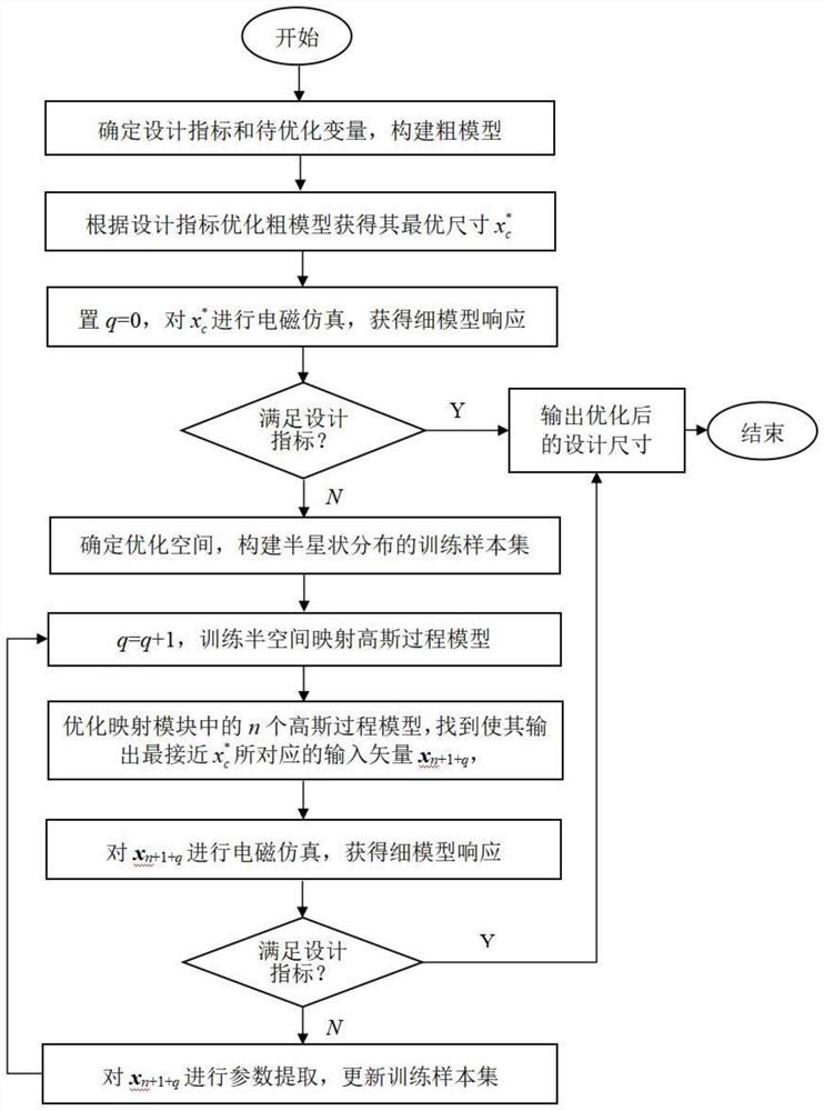
[0033] The optimization process of this embodiment is as follows:

[0034] Step 1: Build an equivalent circuit model in the ADS software, and determine the design index of the microstrip filter. The design index is:

[0035] S 11 ≤-15dB, for 79.2GHz≤f≤83.6GHz

[0036] S 21 ≤-30dB, for 70GHz≤f≤77.4GHz

[0037] S 21 ≤-30dB, for 85.8GHz≤f≤92GHz

[0038] There are six structural variables to be designed, namely L 1 , L 2 , L 3 , S 1 , S 2 , S 3 , written i...


PUM


Abstract

The invention discloses a rapid optimization method for half-space mapping of a microstrip circuit in combination with a Gaussian process, and belongs to the field of computer aided design of microwave radio frequency circuits. The method comprises the following steps: firstly, determining microstrip circuit design indexes and structure variables needing to be optimized, and constructing a rough model; obtaining the optimal design size of the rough model; judging whether the optimal design size of the rough model meets a design index or not, if so, outputting a result and ending the process, otherwise, entering the next step; selecting an initial training sample and a halved optimization space according to semi-star distribution by judging an optimization direction; training a half-space mapping Gaussian process model; the model is optimized, and the optimal result of the next generation is predicted and verified; and if a design index is met, ending the process and outputting an optimization result, otherwise, performing parameter extraction, updating a training set and performing iterative optimization. According to the method, the design efficiency of the microstrip circuit can be improved to a great extent, the number of training samples required by a space mapping technology is reduced, and the convergence speed in the optimization process is accelerated.

Description

technical field [0001] The invention belongs to the field of computer-aided design of microwave radio frequency circuits, and in particular relates to a fast optimization method for half-space mapping of microstrip circuits combined with Gaussian processes. Background technique [0002] Microstrip circuit is a circuit form widely used in various electronic communication devices, and has many advantages such as small size, light weight, high reliability, compact structure, and easy integration. The traditional design of microstrip circuit often needs to rely on the experience of engineers and technicians and electromagnetic simulation software. However, with the development of electronic technology, the design of microstrip circuit structure has been moving towards the direction of miniaturization and high frequency, and various new and complex structures are emerging. It is labor-intensive and labor-intensive to design the circuit structure relying on theory and experience. ...

Claims


Application Information

Patent Timeline
Patent Type & Authority Applications(China)
IPC IPC(8): G06F30/30
CPCG06F30/30
Inventor 喻梦霞汪家兴宁宇航
Owner UNIV OF ELECTRONICS SCI & TECH OF CHINA
Why Eureka
Try Eureka