
Polishing pad, manufacturing method of polishing pad, and manufacturing method of semiconductor device

A manufacturing method and technology of polishing pads, which are applied in the field of polishing pads, can solve the problems such as the increase of concaves on the surface of semiconductor wafers, and achieve the effect of preventing defects and increasing the area of ​​direct contact

Pending Publication Date: 2022-04-12
SK恩普士有限公司
View PDF5 Cites 0 Cited by
  • Summary
  • Abstract
  • Description
  • Claims
  • Application Information

AI Technical Summary

Problems solved by technology

[0007] However, while chemical-mechanical planarization (CMP) polishing using soft pads can improve defects in polished substrates, such pads have the potential to cause increased dishing on metallized semiconductor wafers due to the flexible nature of the pads

Method used


Image

  • Polishing pad, manufacturing method of polishing pad, and manufacturing method of semiconductor device
  • Polishing pad, manufacturing method of polishing pad, and manufacturing method of semiconductor device
  • Polishing pad, manufacturing method of polishing pad, and manufacturing method of semiconductor device

Examples


Embodiment 1

[0215] Manufacturing of Polishing Pads

[0216] Toluene diisocyanate (TDI), dicyclohexylmethane diisocyanate (H 12 MDI), polytetramethylene ether glycol (Polytetramethylene ether glycol) and diethylene glycol (Diethylene glycol) were put into a four-necked flask, and reacted at 80°C for 3 hours to prepare a preform with an NCO% of 8 to 12%. Polymer (Prepolymer).

[0217] In order to manufacture the polishing layer (Top Pad), in the casting machine (Casting Machine) equipped with prepolymer (Prepolymer), curing agent, inert gas injection pipeline and liquid phase foaming agent injection pipeline, the prepared prepolymer (Prepolymer) is filled in the prepolymer tank (Prepolymer Tank), and the curing agent tank is filled with bis (4-amino-3-chlorophenyl) methane (Bis (4-amino-3-chlorophenyl) methane) (Ishihara (Ishihara) company), while preparing nitrogen (N 2 ) was used as an inert gas, and FC3283 (3M company) was prepared as a liquid-phase blowing agent. Unexpanded solid bl...

Embodiment 2

[0223] It was produced in the same manner as in Example 1, except that unexpanded 031DU40 from AkzoNobel was used as the solid-phase blowing agent. The shell (Shell) component of the solid phase foaming agent is polyvinylidene chloride (Polyvinylidene chloride) or acrylonitrile (Acrylonitrile).

Embodiment 3

[0233] Manufacturing of Polishing Pads

[0234] The TDI, H 12 After MDI, polytetramethylene ether glycol (Polytetramethylene ether glycol) and diethylene glycol (Diethylene glycol) were put into a four-necked flask, they were reacted at 80°C for 3 hours to prepare a prepolymer with an NCO% of 8 to 12%. Material (Prepolymer).

[0235] In order to manufacture the polishing layer (Top Pad), in the casting machine (Casting Machine) equipped with prepolymer, curing agent, inert gas injection pipeline and liquid phase foaming agent injection pipeline, fill the prepared prepolymer into the pre polymer tank, and fill bis(4-amino-3-chlorophenyl)methane (Bis(4-amino-3-chlorophenyl)methane) (Ishihara Company) in the curing agent tank, and prepare nitrogen (N 2 ) was used as an inert gas, and FC3283 (3M company) was prepared as a liquid-phase blowing agent.

[0236] The solid-phase blowing agent (AkzoNobel, 551DU40) and the silicon-based surfactant (Evonik) were mixed into the prepolym...


PUM

PropertyMeasurementUnit
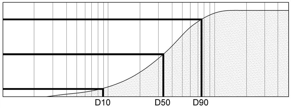
particle sizeaaaaaaaaaa
densityaaaaaaaaaa

Abstract

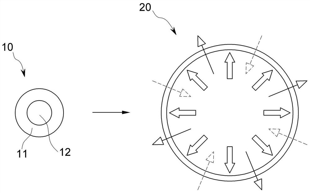
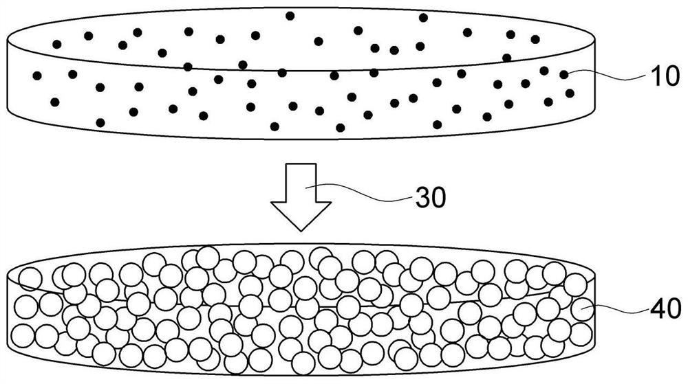
The present invention relates to a polishing pad, a method for manufacturing the polishing pad, and a method for manufacturing a semiconductor device using the polishing pad, for the polishing pad, a polishing composition for manufacturing a polishing layer contains an unexpanded solid-phase foaming agent, and when a curing process is performed, the solid-phase foaming agent expands, and when the curing process is performed, the unexpanded solid-phase foaming agent expands, and when the curing process is performed, the solid-phase foaming agent expands, and the unexpanded solid-phase foaming agent expands, the unexpanded solid-phase foaming agent expands. A plurality of uniform air holes are formed in the polishing layer, so that defects can be prevented from being generated on the surface of the semiconductor substrate. In addition, the invention provides a manufacturing method of the semiconductor device using the polishing pad.

Description

technical field [0001] The invention relates to a polishing pad used in a chemical mechanical planarization (Chemical Mechanical Planarization, CMP) process, a preparation method thereof and a manufacturing method of a semiconductor device using the polishing pad. Background technique [0002] In the chemical mechanical planarization (CMP) process in the semiconductor manufacturing process, the wafer is attached to the head and brought into contact with the surface of the polishing pad formed on the platen, by supplying the slurry It is a process of mechanically flattening the concave-convex part of the wafer surface by using materials to make chemical reactions on the surface of the wafer, and at the same time, moving the platen and the head relative to each other. [0003] After chemical mechanical planarization (CMP) polishing, the metal layer should be parallel or on the same plane as the lower layer of the substrate wafer, but there is also a different "sag" phenomenon....

Claims


Application Information

Patent Timeline
Patent Type & Authority Applications(China)
IPC IPC(8): B24B37/24B24B37/26B24B37/22B24B37/10B24D18/00H01L21/306
CPCB24B37/24B24B7/228B24B37/042H01L21/30625
Inventor 尹钟旭安宰仁郑恩先许惠暎徐章源
Owner SK恩普士有限公司
Learn More