Test access architecture and test access method of digital chip

A digital chip and access method technology, applied in the direction of electronic circuit testing, etc., can solve the problems of large test power consumption, increased wiring overhead, and long test time, and achieve the goal of reducing layout and wiring overhead, reducing test time, and reducing test power consumption Effect

Pending Publication Date: 2022-04-05
BEIJING SMARTCHIP MICROELECTRONICS TECH COMPANY +3
View PDF0 Cites 0 Cited by
  • Summary
  • Abstract
  • Description
  • Claims
  • Application Information

AI Technical Summary

Problems solved by technology

[0003] For the above three test structures, especially when testing large-scale SoC chips, there are the following disadvantages: when the multiplex structure tests all the modules in the SoC chip in series, it is easy to cause the test time to be too long; When all the modules in the SoC chip are tested in parallel, it is easy to cause excessive test power consumption and burn the chip; the daisy chain structure is not easy to design and implement for large-scale SoC chips, and increases wiring overhead

Method used


Image

  • Test access architecture and test access method of digital chip
  • Test access architecture and test access method of digital chip
  • Test access architecture and test access method of digital chip

Examples


Embodiment Construction

[0030] The specific implementation manners of the embodiments of the present invention will be described in detail below in conjunction with the accompanying drawings. It should be understood that the specific implementation manners described here are only used to illustrate and explain the embodiments of the present invention, and are not intended to limit the embodiments of the present invention.

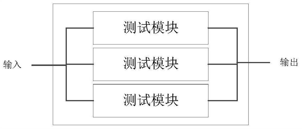
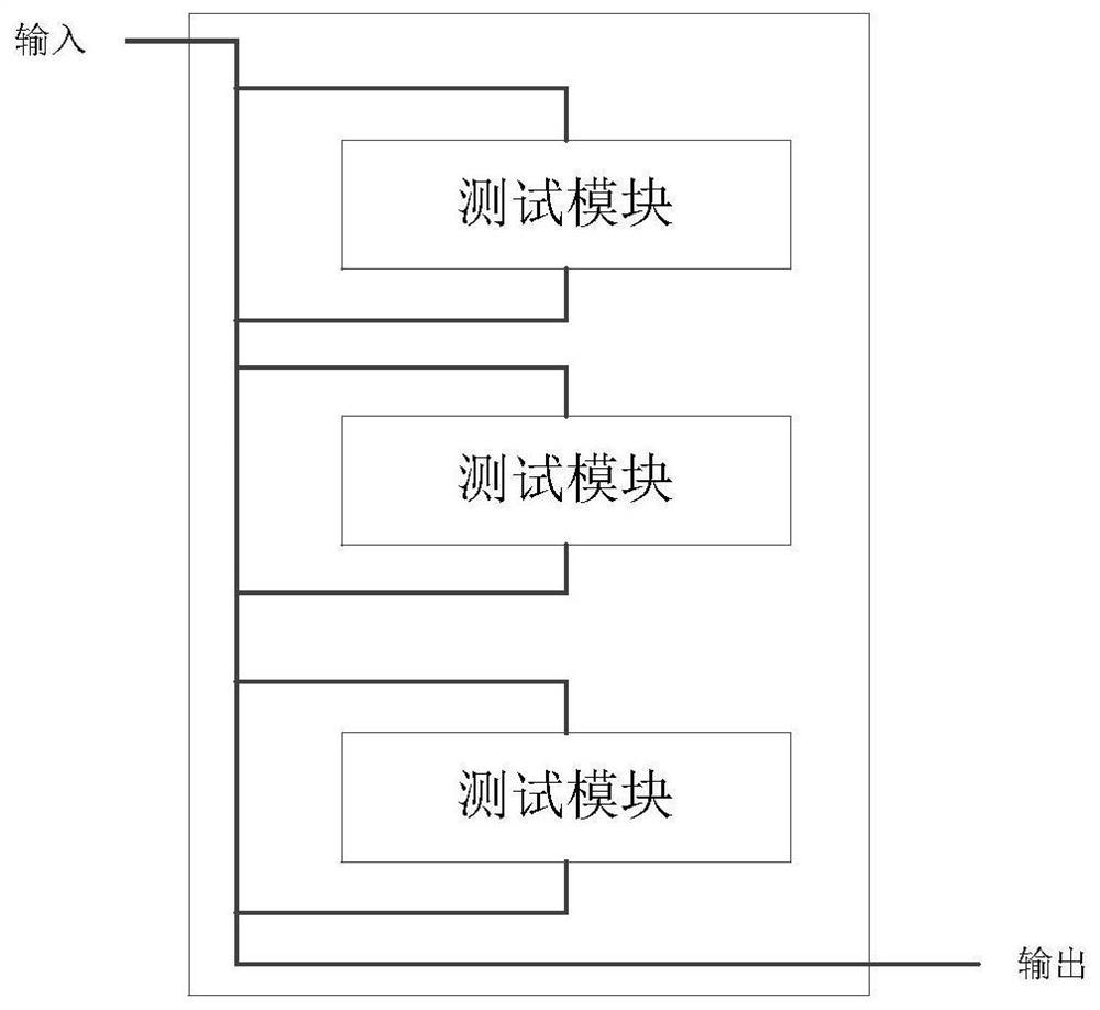
[0031] In the prior art, the multiplex-based test access mechanism belongs to a time-division multiplexing structure, and all modules to be tested are tested serially. by figure 1 The example shown includes the test access structure of three modules to be tested. In order to minimize the test cost, the designer should use the test bandwidth as much as possible to achieve the purpose of reducing the length of the scan chain. Another common test access mechanism is the daisy chain structure, such as figure 2 As shown, in this structure, the scan chain of each module under test i...


PUM


Abstract

The embodiment of the invention provides a test access architecture and a test access method of a digital chip, and belongs to the technical field of integrated circuit testing. The architecture comprises N test groups divided by all modules in a digital chip; wherein each test group in the N test groups comprises a plurality of test modules, and the plurality of test modules in each test group are configured to be tested by adopting a distributed test access mechanism; the N test groups are configured to adopt a multi-path selection test access mechanism for testing. The embodiment of the invention is suitable for architecture division in the test process of large-scale digital chips.

Description

technical field [0001] The invention relates to the technical field of integrated circuit testing, in particular to a test access architecture and a test access method for large-scale digital chips. Background technique [0002] With the rapid development of integrated circuit technology, more and more pure digital chips are applied to various fields. In the current pure digital chips, SoC (System On Chip, System on Chip) chips are designed on a large scale and often contain multiple independent cores. Therefore, when testing SoC chips, it is necessary to test the cores in the SoC chip. Modular testing. At present, there are mainly three test structures for modular testing of SoC chips: multiplex structure, daisy chain structure and distributed structure. [0003] For the above three test structures, especially when testing large-scale SoC chips, there are the following disadvantages: when the multiplex structure tests all the modules in the SoC chip in series, it is easy ...

Claims


Application Information

Patent Timeline
Patent Type & Authority Applications(China)
IPC IPC(8): G01R31/28
Inventor 刘畅李德建李文明王于波冯曦邹华
Owner BEIJING SMARTCHIP MICROELECTRONICS TECH COMPANY
Why Eureka
Try Eureka