Method, device and equipment for testing bad storage unit of flash memory and storage medium
A storage unit and test method technology, applied in static memory, instruments, etc., can solve problems such as no technical solution and low test efficiency, and achieve the effect of reducing object base, reducing useless information, and simplifying judgment logic
- Summary
- Abstract
- Description
- Claims
- Application Information
AI Technical Summary
Problems solved by technology
Method used
Image

Examples
Embodiment 1
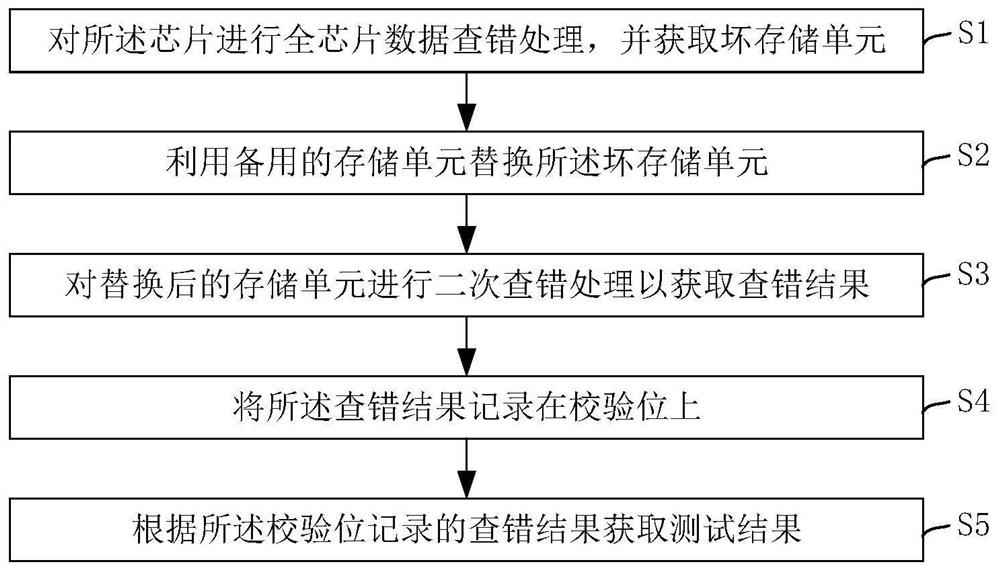
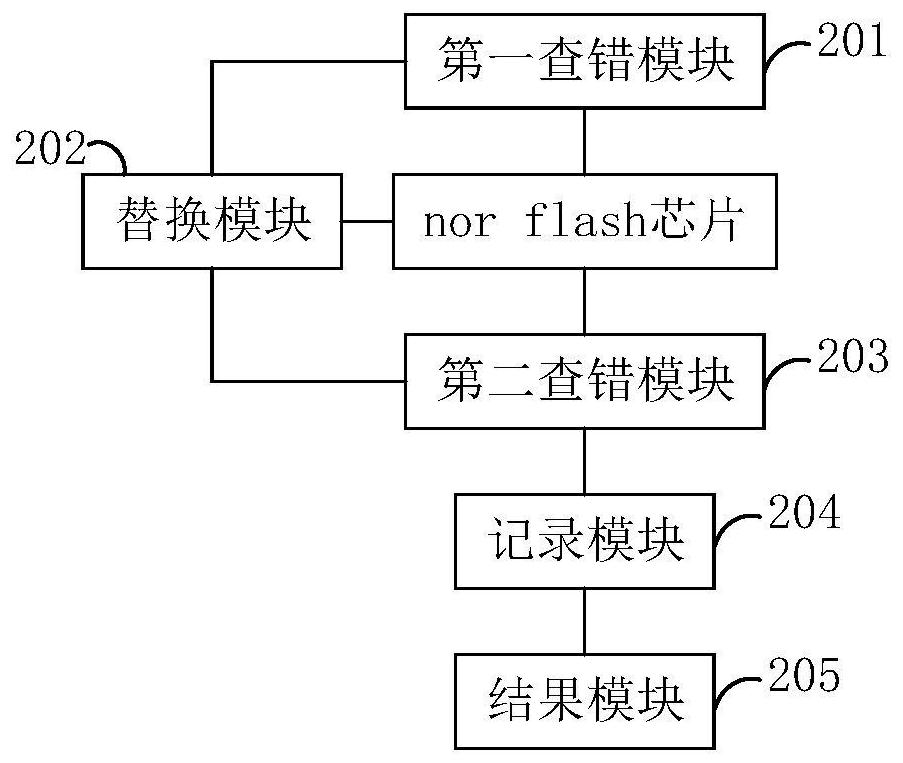
[0083] Start the bad memory unit test item test for a nor flash chip, first write all 0 data into the chip, and set a check digit at the same time, the check digit data is 0, and then use 8 bytes of data as the error checking unit from the beginning start address to start reading the data in the chip.
[0084]Verify that the read 8-byte data is all 0, if so, read and verify the data of the next 8-byte address; if not, it indicates that the storage unit corresponding to the 8-byte address is a bad storage unit , at this time, call the spare storage unit corresponding to the 8-byte address from the chip redundancy area to replace the bad storage unit in the form of mapping, and then check whether the 8-byte data in the replaced storage unit is all 0 , if yes, then read and verify the data of the next 8-byte address, if not, it indicates that the replaced storage unit is still a bad storage unit, at this time, a verification error signal is output, and the verification bit data i...
Embodiment 2
[0088] Start the bad memory unit test item test for a nor flash chip, first write all 0 data into the chip, and set a check digit at the same time, the check digit data is 0, and then use 8 bytes of data as the error checking unit from the beginning start address to start reading the data in the chip.
[0089] Verify that the read 8-byte data is all 0, if so, read and verify the data of the next 8-byte address; if not, it indicates that the storage unit corresponding to the 8-byte address is a bad storage unit , at this time, call the spare storage unit corresponding to the 8-byte address from the chip redundancy area to replace the bad storage unit in the form of mapping, and then check whether the 8-byte data in the replaced storage unit is all 0 , if yes, then read and verify the data of the next 8-byte address, if not, it indicates that the replaced storage unit is still a bad storage unit, at this time, a verification error signal is output, and the verification bit data ...
Embodiment 3
[0093] Start the bad memory unit test item test for a nor flash chip, first write all 0 data into the chip, and set a check digit at the same time, the check digit data is 0, and then use 8 bytes of data as the error checking unit from the beginning start address to start reading the data in the chip.
[0094] Verify that the read 8-byte data is all 0, if so, read and verify the data of the next 8-byte address; if not, it indicates that the storage unit corresponding to the 8-byte address is a bad storage unit , record the address of the bad storage unit, and then read and verify the data of the next 8-byte address; after the data reading and verification of the last 8-byte address of the chip is completed, the bad memory unit with the recorded address is read one by one. The storage unit performs the following operations: call the spare storage unit corresponding to the 8-byte address from the redundant area of the chip to replace the bad storage unit in the form of mapping...
PUM
 Abstract
Description
Claims
Application Information
 - R&D Engineer
- R&D Manager
- IP Professional
- Industry Leading Data Capabilities
- Powerful AI technology
- Patent DNA Extraction
Browse by: Latest US Patents, China's latest patents, Technical Efficacy Thesaurus, Application Domain, Technology Topic.
© 2024 PatSnap. All rights reserved.Legal|Privacy policy|Modern Slavery Act Transparency Statement|Sitemap