Area-friendly storage address mapping method for systolic array

A technique of pulsating arrays and storing addresses, applied in memory systems, instruments, electrical digital data processing, etc., can solve problems such as ratio reduction and complex address lines

Pending Publication Date: 2022-03-22
NAT UNIV OF DEFENSE TECH
View PDF0 Cites 0 Cited by
  • Summary
  • Abstract
  • Description
  • Claims
  • Application Information

AI Technical Summary

Problems solved by technology

The main reason is that in hardware design, the greater the depth of the memory bank, the more complex the address lines required for pseudo-dual-port TP storage, which also leads to the continuous expansion of pseudo-dual-port TP storage and single-port SP storage.
However, when the depth reaches a certain value, although the single-port SP saves a larger area than the pseudo-dual-port TP, the ratio shrinks instead.

Method used


Image

  • Area-friendly storage address mapping method for systolic array
  • Area-friendly storage address mapping method for systolic array
  • Area-friendly storage address mapping method for systolic array

Examples


Embodiment Construction

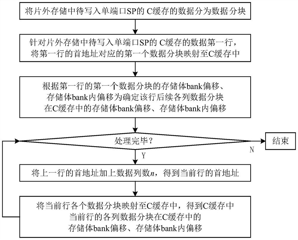
[0044] The purpose of the area-friendly storage address mapping method oriented to systolic arrays in the present invention is to optimize the on-chip area of ​​the systolic accelerator, and to reduce the area cost of the on-chip memory as much as possible in terms of on-chip storage under the premise of ensuring operation efficiency and calculation accuracy. The area-friendly storage address mapping method oriented to systolic arrays of the present invention will be further described in detail below with reference to examples.

[0045] Such as figure 1 As shown, the area-friendly memory address mapping method for systolic arrays in this embodiment includes:

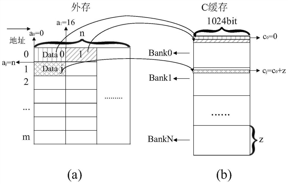
[0046] 1) The data to be written into the C cache of the single-port SP in the off-chip storage is divided into data blocks (block);

[0047] 2) For the first row of data to be written into the C cache of the single-port SP in the off-chip storage, set the first address a of the first row 0 The corresponding first dat...


PUM


Abstract

The invention discloses a systolic array-oriented area-friendly memory address mapping method. The method comprises the following steps of: dividing data to be written into a C cache of a single port SP in an off-chip memory into data blocks; the method comprises the following steps of: traversing data to be written into a C cache of a single port SP in an off-chip memory by taking a row as a unit, and respectively mapping each data block of a current row into the C cache to obtain a memory bank offset cji0 and a memory bank internal offset cji1 of each column of data blocks cji of a current row cj in the C cache in the C cache. According to the advantages and disadvantages of the single-port SP, high-efficiency address translation based on the single-port SP can be realized, and under the condition that the access behavior of the intermediate result in the operation process of the pulsating accelerator is not influenced, address mapping of data stored in the intermediate result written from the outside of a chip is changed, so that the purpose of reducing the area of a memory bank is achieved.

Description

technical field [0001] The invention relates to data storage technology, in particular to an area-friendly storage address mapping method oriented to a systolic array. Background technique [0002] Since the emergence of deep learning, people's lives have undergone earth-shaking changes, and the idea of ​​​​developing a dedicated chip for neural networks has long been deeply rooted in the hearts of the people. In 2013, various products and services provided by Google, such as Google Image Search, Google Photos, Google Cloud Vision API, and Google Translate, required the use of deep neural networks. Under the huge application scale, Google internally realized that these millions of servers running day and night, their internal fast-growing computing needs made it necessary to double the number of data centers to be satisfied. However, no matter in terms of cost or computing power, the internal center can no longer simply rely on GPU and CPU to maintain, which also promotes t...

Claims


Application Information

Patent Timeline
Patent Type & Authority Applications(China)
IPC IPC(8): G06F12/1009G06F12/1045
CPCG06F12/1009G06F12/1045Y02D10/00
Inventor 文梅杨韧禹沈俊忠曹亚松张洋刘胜
Owner NAT UNIV OF DEFENSE TECH
Why Eureka
Try Eureka