Printing circuit board defective image allocation methods, devices, equipment and storage media

A printed circuit board, image registration technology, applied in the field of defect detection, can solve the problem of low image registration accuracy, and achieve the effect of improving accuracy and reducing the influence of interference factors

Active Publication Date: 2022-05-13
北京阿丘科技有限公司
View PDF0 Cites 0 Cited by
  • Summary
  • Abstract
  • Description
  • Claims
  • Application Information

AI Technical Summary

Problems solved by technology

[0004] The main purpose of the present invention is to provide a printed circuit board defect image registration method, device, equipment and storage medium, aiming to solve the technical problem of low accuracy of image registration in the prior art

Method used


Image

  • Printing circuit board defective image allocation methods, devices, equipment and storage media
  • Printing circuit board defective image allocation methods, devices, equipment and storage media
  • Printing circuit board defective image allocation methods, devices, equipment and storage media

Examples


Embodiment Construction

[0050] It should be understood that the specific embodiments described here are only used to explain the present invention, not to limit the present invention.

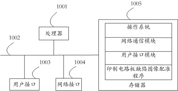
[0051] refer to figure 1 , figure 1 It is a schematic structural diagram of a printed circuit board defect image registration device related to the hardware operating environment of the embodiment of the present invention.

[0052] Such as figure 1As shown, the printed circuit board defect image registration device may include: a processor 1001 , such as a central processing unit (Central Processing Unit, CPU), a communication bus 1002 , a user interface 1003 , a network interface 1004 , and a memory 1005 . Wherein, the communication bus 1002 is used to realize connection and communication between these components. The user interface 1003 may include a display screen (Display), an input unit such as a keyboard (Keyboard), and the optional user interface 1003 may also include a standard wired interface and a wireles...


PUM


Abstract

The invention discloses a printed circuit board defect image registration method, device, equipment and storage medium. The method includes: obtaining a product picture and a preset template picture of a printed circuit board; Points are matched with the corresponding non-deformable key points in the preset template image to determine several non-deformable registration positions; several deformable key points in the product image are matched with the corresponding deformable key points in the preset template image, to determine a number of deformable registration areas; perform image transformation on the product picture according to the number of non-deformable registration positions and the number of deformable registration areas, and obtain a defect registration image of the printed circuit board. The invention reduces the influence of interference factors and improves the accuracy of defect registration images by separately matching non-deformable key points and deformable key points.

Description

technical field [0001] The present invention relates to the technical field of defect detection, in particular to a method, device, equipment and storage medium for defect image registration of printed circuit boards. Background technique [0002] When classifying the defect images of printed circuit boards, it is necessary to register the defective product images generated in real time with the template images drawn according to the design files to obtain registration images, so as to classify the defect images according to the registration images , the accuracy of the registration image determines the accuracy of the defect image classification. The existing image registration methods are greatly affected by interference factors, resulting in low registration accuracy. Therefore, how to improve the accuracy of image registration has become an urgent technology to be solved. question. [0003] The above content is only used to assist in understanding the technical solution...

Claims


Application Information

Patent Timeline
Patent Type & Authority Patents(China)
IPC IPC(8): G06T7/00G06T7/13G06T7/33G06N3/04G06N3/08
CPCG06T7/0004G06T7/13G06T7/337G06N3/08G06T2207/20081G06T2207/20084G06T2207/20164G06T2207/30141G06N3/045
Inventor 黄耀陈天玓
Owner 北京阿丘科技有限公司
Why Eureka
Try Eureka