Production method of refrigeration infrared detector

An infrared detector and device chip technology, which is applied in the field of semiconductors and can solve the problems that the physical connection and electrical connection between a readout circuit chip and a device chip cannot meet process requirements, device failure, indium column dislocation, etc.

Pending Publication Date: 2022-02-18
ZHEJIANG JUEXIN MICROELECTRONICS CO LTD
View PDF0 Cites 0 Cited by
  • Summary
  • Abstract
  • Description
  • Claims
  • Application Information

AI Technical Summary

Problems solved by technology

[0005] The purpose of the present invention is to provide a method for preparing a refrigerated infrared detector, so as to solve the problem of dislocation and sideslip of the indium column after the readout circuit chip and the device chip used to form the refrigerated infrared detector are flip-bonded, which leads to the readout circuit chip The physical connection and electrical connection with the device chip cannot meet the process requirements, and eventually cause the problem of device failure

Method used


Image

  • Production method of refrigeration infrared detector
  • Production method of refrigeration infrared detector
  • Production method of refrigeration infrared detector

Examples


preparation example Construction

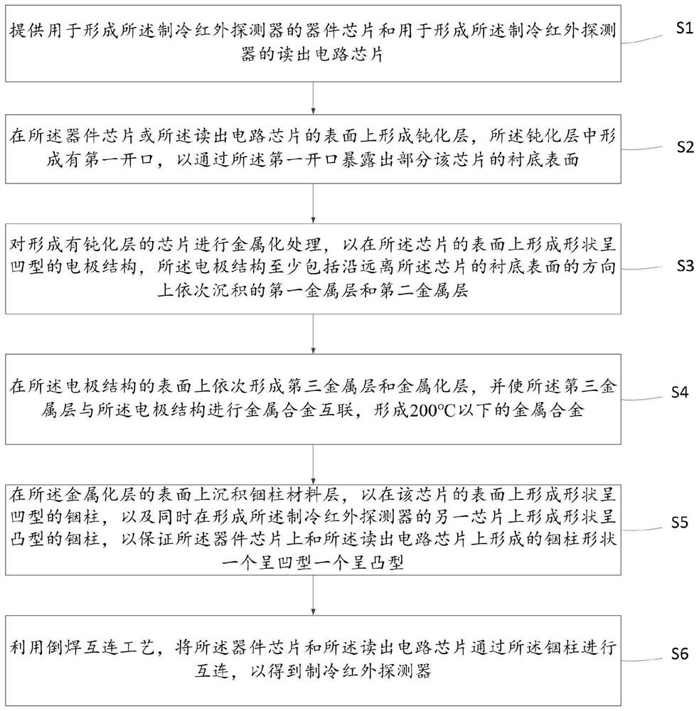
[0040] refer to figure 1 , figure 1 It is a schematic flow chart of a method for preparing a cooled infrared detector in an embodiment of the present invention provided in an embodiment of the present invention, and the method includes the following steps:

[0041] Step S1, providing a device chip for forming the cooled infrared detector and a readout circuit chip for forming the cooled infrared detector;

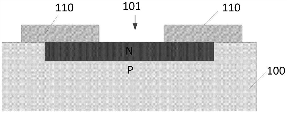
[0042] Step S2, forming a passivation layer on the surface of the device chip or the readout circuit chip, a first opening is formed in the passivation layer, so as to expose part of the substrate of the chip through the first opening surface;

[0043] S3, performing metallization treatment on the chip formed with the passivation layer, so as to form a concave electrode structure on the surface of the chip, the electrode structure at least includes sequentially along the direction away from the substrate surface of the chip Deposited first metal layer and second metal la...


PUM


Abstract

The invention provides a production method of a refrigeration infrared detector, which is applied to the technical field of semiconductors. Specifically, a concave or convex indium column is formed on a device chip or a reading circuit chip which forms the refrigeration infrared detector, and then, under the condition that the shape of the indium column of the chip on which the concave indium column is formed is kept unchanged, the indium column of the chip with the convex indium column is melted after being heated and then is connected with the indium column of the chip with the concave indium column in a face-down bonding mode so that a cold-hot face-down bonding mode (the specific implementation can be determined to be cold at the upper part and hot at the lower part, or hot at the lower part and cold at the upper part, and the temperature of the cold end is generally 0-30 DEG C, and the temperature of the hot end is generally 80-250 DEG C) is adopted. The purposes of enhancing the stability of the indium column, avoiding sideslip and offset of the indium column and ensuring that the indium column is not prone to falling off and deformation are achieved, physical connection and electrical connection of the reading circuit chip and the device chip can meet the process requirements, and finally the problem of the device is solved.

Description

technical field [0001] The invention relates to the technical field of semiconductors, in particular to a preparation method of a cooling infrared detector. Background technique [0002] With the continuous promotion and development of infrared applications, advanced infrared detection technology requires detectors to have higher spatial resolution and better target recognition capabilities. Infrared detector is a photoelectric device that converts infrared radiation into electronic signals, in which the photoelectric reaction is only carried out on the photosensitive element, and the subsequent signal processing process only involves electronic technology, so the infrared detection chip is the core of the infrared detector. core components. Since the current CMOS integrated circuit technology is mainly based on the Si process, the infrared detection chip needs to be mixed and integrated with the Si readout circuit through the indium column flip-chip interconnection technol...

Claims


Application Information

Patent Timeline
Patent Type & Authority Applications(China)
IPC IPC(8): H01L27/146
CPCH01L27/1469H01L27/14687H01L27/14632H01L27/14634H01L27/14636
Inventor 毛剑宏杜宇杨天伦
Owner ZHEJIANG JUEXIN MICROELECTRONICS CO LTD
Why Eureka
Try Eureka