
Diode

A diode and cathode structure technology, applied in the diode field, can solve problems such as low reliability, and achieve the effects of improving reliability, improving sturdiness, and reducing the magnitude of static breakdown voltage reduction.

Pending Publication Date: 2022-01-21
BEIJING UNIV OF TECH +2
View PDF6 Cites 0 Cited by
  • Summary
  • Abstract
  • Description
  • Claims
  • Application Information

AI Technical Summary

Problems solved by technology

[0005] In order to overcome the deficiency of low reliability in the above-mentioned prior art, the present invention provides a diode, comprising an N-type substrate (1), an anode structure (3) and a cathode structure (2), and the anode structure (3) is located on the N-type substrate On the front side of the bottom (1), the cathode structure (2) is located on the back side of the N-type substrate (1);

Method used


Image

  • Diode
  • Diode
  • Diode

Examples


Embodiment Construction

[0037] The present invention will be described in further detail below in conjunction with the accompanying drawings.

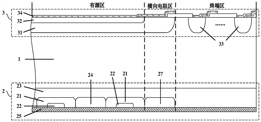
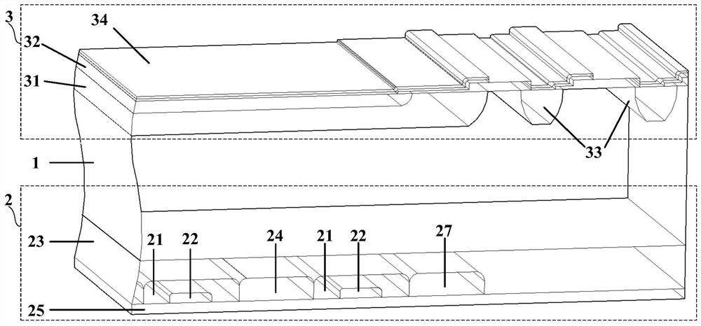
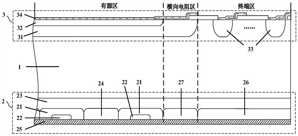
[0038] The embodiment of the present invention provides a diode, including an N-type substrate 1, an anode structure 3 and a cathode structure 2, the anode structure 3 is located on the front of the N-type substrate 1, and the cathode structure 2 is located on the back of the N-type substrate.

[0039] Such as figure 1 and figure 2 As shown, the cathode structure 2 includes at least one first P+ doped layer 21 and a first N+ doped layer 22 located in the middle of each first P+ doped layer 21 .

[0040] The cathode structure 2 further includes at least one second N+ doped layer 24 ; at least one first P+ doped layer 21 and at least one second N+ doped layer 24 are arranged at intervals.

[0041] The cathode structure 2 also includes an N-type buffer layer 23 and a cathode electrode 25;

[0042] The N-type buffer layer 23 is located between the back of the...


PUM

PropertyMeasurementUnit
widthaaaaaaaaaa
widthaaaaaaaaaa

Abstract

The invention provide s a diode which comprises an N-type substrate, an anode structure and a cathode structure, the anode structure is located on the front surface of the N-type substrate, and the cathode structure is located on the back surface of the N-type substrate. The cathode structure comprises at least one first P + doping layer and a first N + doping layer located in each first P + doping layer, the on-state voltage drop of the diode can be greatly reduced through the first N + doping layers, the reduction amplitude of a static breakdown voltage can be reduced, and the reliability of the diode is improved. According to the invention, the third N + doping layer is arranged in the transverse resistance region in the N-type buffer layer so that the accumulation amount of carriers at the edge of an active region when the diode is switched on is effectively suppressed, namely, the current concentration at the edge of the inner side of the diode at the initial turn-off stage is suppressed, the current filament at the final turn-off stage is dispersed, the over-current turn-off firmness of the diode is remarkably improved, the capability of inhibiting high dynamic avalanche of the diode is improved, and burnout caused by direct formation of a through current wire between the first P + doping layer and the edge of the active region at the end of reverse recovery is effectively avoided.

Description

technical field [0001] The invention relates to the technical field of semiconductors, in particular to a diode. Background technique [0002] Diodes have the advantages of small forward conduction resistance, high reverse blocking voltage, and short recovery time, and are widely used in high-speed trains, new energy vehicles, and smart grids. Due to the asymmetry of the diode's own structure and the fact that the diode may work under harsh electrical stress conditions, the diode is easily burned due to the dynamic avalanche phenomenon during the turn-off process. [0003] In order to make the diode have a high dynamic avalanche suppression capability, it is usually necessary to inject a controllable hole (Controlled Injection of Backside Holes, CIBH) structure on the cathode side of the diode, so that the diode injects holes into the N-drift region during reverse recovery to The electrons generated by the dynamic avalanche are compensated, and the strong electric field on ...

Claims


Application Information

Patent Timeline
Patent Type & Authority Applications(China)
IPC IPC(8): H01L29/861H01L29/06
CPCH01L29/861H01L29/0619
Inventor 王立昊吴郁刘钺杨金锐孙国繁高晋文王克胜
Owner BEIJING UNIV OF TECH
Learn More