
Two-dimensional rhenium sulfide photoelectric detector and preparation method thereof

A photodetector, rhenium sulfide technology, applied in circuits, electrical components, semiconductor devices, etc., can solve the problem of slow response time of photodetectors, and achieve the effect of high responsivity

Pending Publication Date: 2022-01-14
HANGZHOU DIANZI UNIV
View PDF0 Cites 0 Cited by
  • Summary
  • Abstract
  • Description
  • Claims
  • Application Information

AI Technical Summary

Problems solved by technology

However, the existence of a large number of defect states will make the ReS 2 The response time of photodetectors is usually slow (on the order of minutes)

Method used


Image

  • Two-dimensional rhenium sulfide photoelectric detector and preparation method thereof
  • Two-dimensional rhenium sulfide photoelectric detector and preparation method thereof
  • Two-dimensional rhenium sulfide photoelectric detector and preparation method thereof

Examples


Embodiment Construction

[0032] The technical solutions provided by the present invention will be further described below in conjunction with the accompanying drawings.

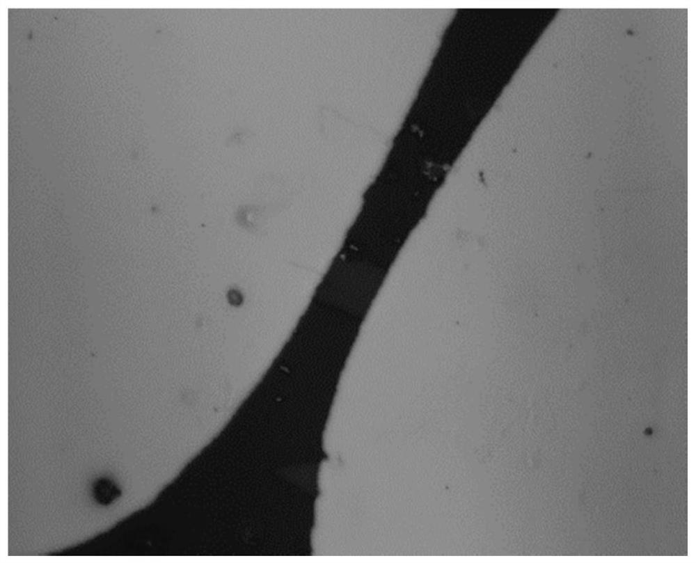
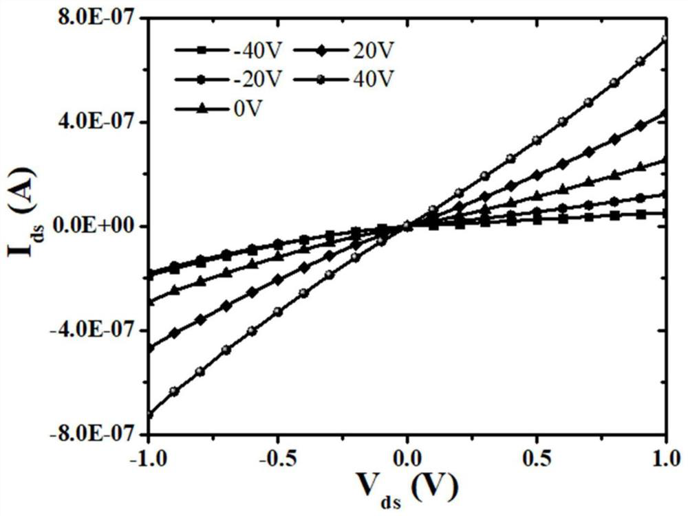
[0033] see figure 1 , which is a schematic structural view of the two-dimensional rhenium sulfide photodetector of the present invention, which at least includes a substrate layer (1) and an insulating layer (2) formed on the substrate layer (1), and the insulating layer (2) is set A two-dimensional rhenium sulfide layer (4), and an electrode (3) connected to the two-dimensional rhenium sulfide layer (4) is set as a source and a drain, and the two-dimensional rhenium sulfide layer (4) is doped A tetracyanodimethyl-p-benzoquinone layer (5) is formed. The present invention adopts macromolecule F 4 -TCNQ performs surface doping on the two-dimensional rhenium sulfide layer (4) to form a tetracyanodimethyl-p-benzoquinone layer (5), thereby obtaining doped F 4 - ReS of TCNQ 2 light detector. see figure 2 , shows the optical picture ...


PUM

PropertyMeasurementUnit
Thicknessaaaaaaaaaa
Thicknessaaaaaaaaaa

Abstract

The invention discloses a two-dimensional rhenium sulfide photoelectric detector and a preparation method, the two-dimensional rhenium sulfide photoelectric detector at least comprises a substrate layer and an insulating layer formed on the substrate layer, a two-dimensional rhenium sulfide layer is arranged on the insulating layer, and electrodes connected with the two-dimensional rhenium sulfide layer are arranged as a source electrode and a drain electrode. And a tetracyanodimethyl p-benzoquinone layer is formed on the two-dimensional rhenium sulfide layer through doping. ReS2 is subjected to surface modification through macromolecule F4-TCNQ to regulate and control the performance of the ReS2, and the ReS2 photoelectric detector with multiple performance combinations is obtained and comprises a high-responsivity and high-sensitivity ReS2 photoelectric detector.

Description

technical field [0001] The invention relates to the field of optoelectronic devices, in particular to a two-dimensional rhenium sulfide photodetector and a preparation method. Background technique [0002] Two-dimensional transition metal dichalcogenides (TMDs) have attracted extensive attention from the scientific community due to their unique electrical and optical properties. Since the size of TMDs is generally only a few nanometers, it is considered one of the feasible solutions to continue Moore's Law. At present, many studies have proved that it can be applied to optoelectronic semiconductor functional devices such as photodetectors, logic circuits, sensors, and memristors. Photodetectors based on TMDs, as basic optoelectronic devices, were once widely studied. For example, mechanical exfoliation of monolayer MoS 2 Phototransistor with a responsivity of 880A / W in the electron depletion region; 3 layers of WSe 2 Ultra-fast photodetector, the responsivity reaches 7A / ...

Claims


Application Information

Patent Timeline
IPC IPC(8): H01L31/032H01L31/102H01L31/18
CPCH01L31/0321H01L31/102H01L31/18Y02P70/50
Inventor 吴章婷曾培宇张阳郑鹏郑梁
Owner HANGZHOU DIANZI UNIV
Learn More