
Tellurium semiconductor film infrared detection device

An infrared detector and semiconductor technology, applied in the field of infrared detection, can solve the problem that Te short-wave infrared detectors are difficult to take into account dark current, responsivity and CMOS compatibility, and achieve the effect of low cost, low dark current and good compatibility

Pending Publication Date: 2021-12-31
HUAZHONG UNIV OF SCI & TECH
View PDF0 Cites 0 Cited by
  • Summary
  • Abstract
  • Description
  • Claims
  • Application Information

AI Technical Summary

Problems solved by technology

[0004] The invention provides a tellurium semiconductor thin-film infrared detection device, which can solve the technical problem that current Te short-wave infrared detectors are difficult to take into account dark current, responsivity and CMOS compatibility

Method used


Image

  • Tellurium semiconductor film infrared detection device
  • Tellurium semiconductor film infrared detection device

Examples


Embodiment Construction

[0024] The present invention is described in detail below in conjunction with examples, but the present invention is not limited to these examples.

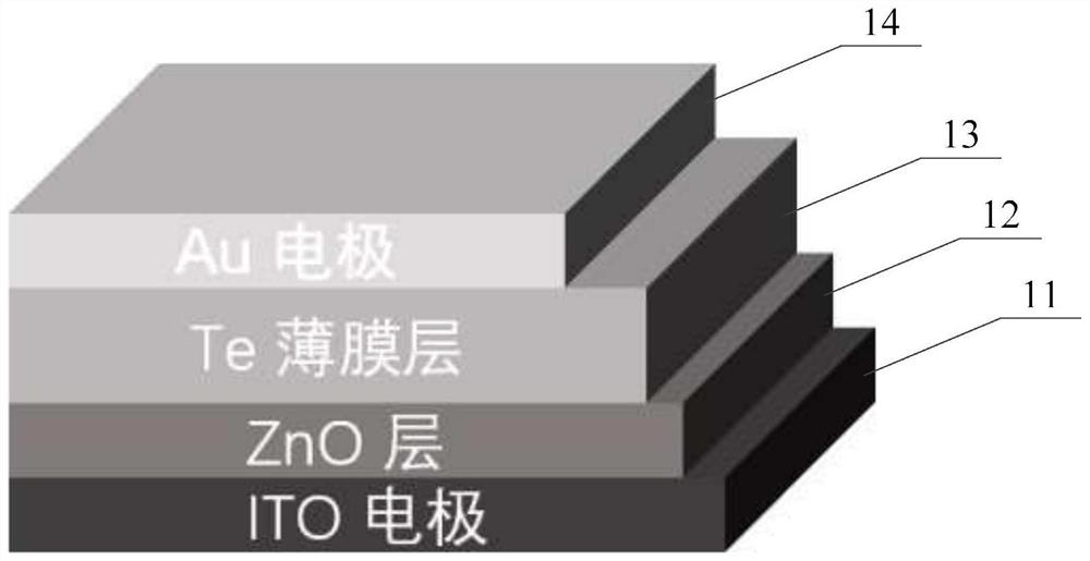
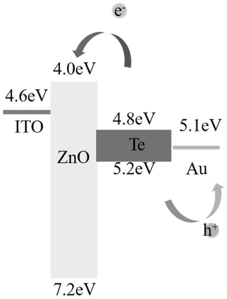
[0025] Although Te single crystals and devices have achieved good detection performance, they cannot be integrated in CMOS; micro-nano devices have also achieved high device performance, but the dark current is large, the noise is large, and the specific detection rate is small. The signal-to-noise ratio is poor, and it is difficult to realize large-scale production and area array imaging applications; the dark current of the thin film field effect tube device is small, but the film is thin and the light absorption is insufficient, so the sensitivity is poor, and the technology and CMOS compatibility are poor, so the present invention is based on Based on the device structure design, it solves the key problem of Te short-wave infrared detector taking into account dark current, responsivity and CMOS compatibility.

[0026] Specifi...


PUM

PropertyMeasurementUnit
thicknessaaaaaaaaaa
thicknessaaaaaaaaaa
thicknessaaaaaaaaaa

Abstract

The invention discloses a tellurium semiconductor film infrared detection device, belongs to the technical field of infrared detection, and can solve the technical problem that a current Te short wave infrared detector is difficult to consider dark current, responsivity and CMOS compatibility. The tellurium semiconductor film infrared detection device comprises a first electrode which is a transparent electrode, an electron transport layer disposed on the first electrode, a tellurium film layer arranged on the electron transport layer, and a second electrode arranged on the tellurium film layer. The device is used for manufacturing the infrared detector.

Description

technical field [0001] The invention relates to a tellurium semiconductor thin film infrared detection device, which belongs to the technical field of infrared detection. Background technique [0002] Tellurium (Te) is a new short-wave infrared detection material, which has the advantages of low raw material cost, excellent photoelectric properties of non-toxic antibacterial agent, and has great potential to realize high-performance infrared detection. In the 1950s, researchers began to pay attention to the infrared detection application of Te, but most of them were Te single-crystal infrared detection devices, which were not conducive to the application of CMOS integration and actual imaging. [0003] Te thin film devices have better compatibility with CMOS, but the research on Te thin film infrared photodetectors has just started. At present, the infrared detection application of Te thin film is limited to the short-wave infrared field effect transistor of Te thin film. ...

Claims


Application Information

Patent Timeline
Patent Type & Authority Applications(China)
IPC IPC(8): H01L31/109H01L31/18C23C14/06C23C14/08C23C14/24C23C14/35
CPCH01L31/109H01L31/18C23C14/086C23C14/35C23C14/24C23C14/06
Inventor 唐江付刘冲陈超郑佳佳鲁帅成刘婧
Owner HUAZHONG UNIV OF SCI & TECH
Learn More