Electric floating silicon distortionless heterogeneous DEHFET device and preparation method thereof
A distortion-free and heterogeneous technology, applied in semiconductor/solid-state device manufacturing, electrical components, semiconductor devices, etc., can solve problems such as failure to work normally, device failure, etc., to reduce thermal charges, reduce transient currents, and reduce electron collection Effect
- Summary
- Abstract
- Description
- Claims
- Application Information
AI Technical Summary
Problems solved by technology
Method used
Image
Examples
Embodiment 1
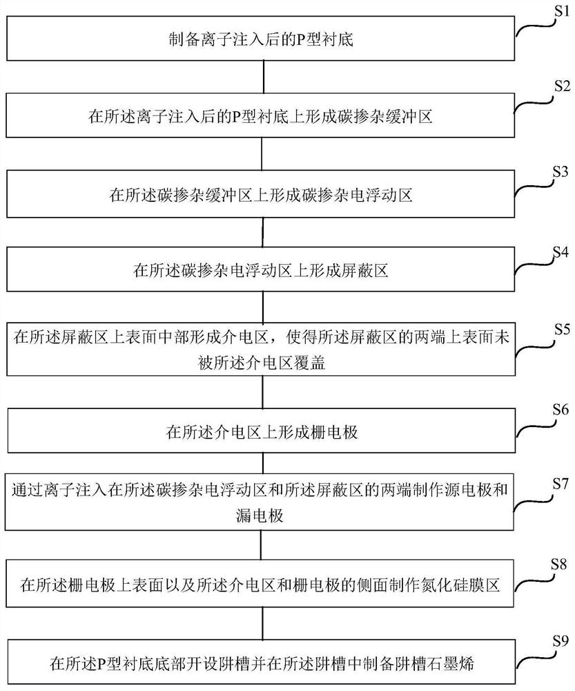
[0051] See figure 1 ,Please refer to figure 1 and Figure 2a to Figure 2i , figure 1 It is a flow chart of a method for preparing an electrically floating silicon distortion-free heterogeneous DEHFET device provided by an embodiment of the present invention; Figure 2a to Figure 2iIt is a schematic diagram of the preparation process of an electrically floating silicon distortion-free heterogeneous DEHFET device provided by an embodiment of the present invention. The preparation method of this DEHFET device comprises:
[0052] Step 1, see Figure 2a , preparing an ion-implanted P-type substrate 1 .
[0053] Step 1.1. Select a P-type lightly doped silicon substrate 1 .
[0054] Wherein, the thickness range of the P-type lightly doped silicon substrate 1 is 305-405 um.
[0055] Step 1.2, implanting boron ions into the P-type lightly doped silicon substrate 1, and performing annealing treatment after the boron ion implantation is completed, so as to obtain the P-type substr...
Embodiment 2
[0095] This embodiment provides an electrically floating silicon distortion-free heterogeneous DEHFET device on the basis of the above embodiments. See image 3 , image 3 It is a schematic structural diagram of an electrically floating silicon distortion-free heterogeneous DEHFET device provided by an embodiment of the present invention. The electric floating silicon distortion-free heterogeneous DEHFET device includes a P-type substrate 1, a carbon-doped buffer zone 2, a carbon-doped electric floating region 3, a shielding region 4, a dielectric region 5, a gate electrode 6, a source electrode 7, a drain electrode electrode 8, silicon nitride film region 9 and well-grooved graphene 10.
[0096] P-type substrate 1, carbon-doped buffer zone 2, carbon-doped electric floating region 3, shielding region 4, dielectric region 5 and gate electrode 6 are arranged in sequence from bottom to top, and dielectric region 5 covers the shielding region 4 The middle part, so that part of ...
PUM
| Property | Measurement | Unit |
|---|---|---|
| thickness | aaaaa | aaaaa |
| thickness | aaaaa | aaaaa |
| thickness | aaaaa | aaaaa |
Abstract
Description
Claims
Application Information
 - R&D
- Intellectual Property
- Life Sciences
- Materials
- Tech Scout
- Unparalleled Data Quality
- Higher Quality Content
- 60% Fewer Hallucinations
Browse by: Latest US Patents, China's latest patents, Technical Efficacy Thesaurus, Application Domain, Technology Topic, Popular Technical Reports.
© 2025 PatSnap. All rights reserved.Legal|Privacy policy|Modern Slavery Act Transparency Statement|Sitemap|About US| Contact US: help@patsnap.com


