Construction method of curved surface honeycomb array and application of curved surface honeycomb array

An array structure and honeycomb structure technology, applied in the field of nanocomposite materials, can solve the problems of lack of manufacturable structure change space, insufficient application field, harsh test conditions, etc. Repeatable effects

Pending Publication Date: 2021-11-16
HANGZHOU DIANZI UNIV
View PDF12 Cites 0 Cited by
  • Summary
  • Abstract
  • Description
  • Claims
  • Application Information

AI Technical Summary

Problems solved by technology

[0009] In order to overcome the disadvantages of the prior art, such as insufficiently wide application field of the ordered nanostructure active substrate, cumbersome construction steps, long preparation period, high cost, harsh test conditions, and lack of space for changing the manufacturable structure, the present invention provides A method for constructing a curved honeycomb structure with rich structures and applications has opened up the operable space of nanostructures in the future and enriched the application fields of nanostructures in the future.

Method used


Image

  • Construction method of curved surface honeycomb array and application of curved surface honeycomb array
  • Construction method of curved surface honeycomb array and application of curved surface honeycomb array
  • Construction method of curved surface honeycomb array and application of curved surface honeycomb array

Examples


Embodiment 1

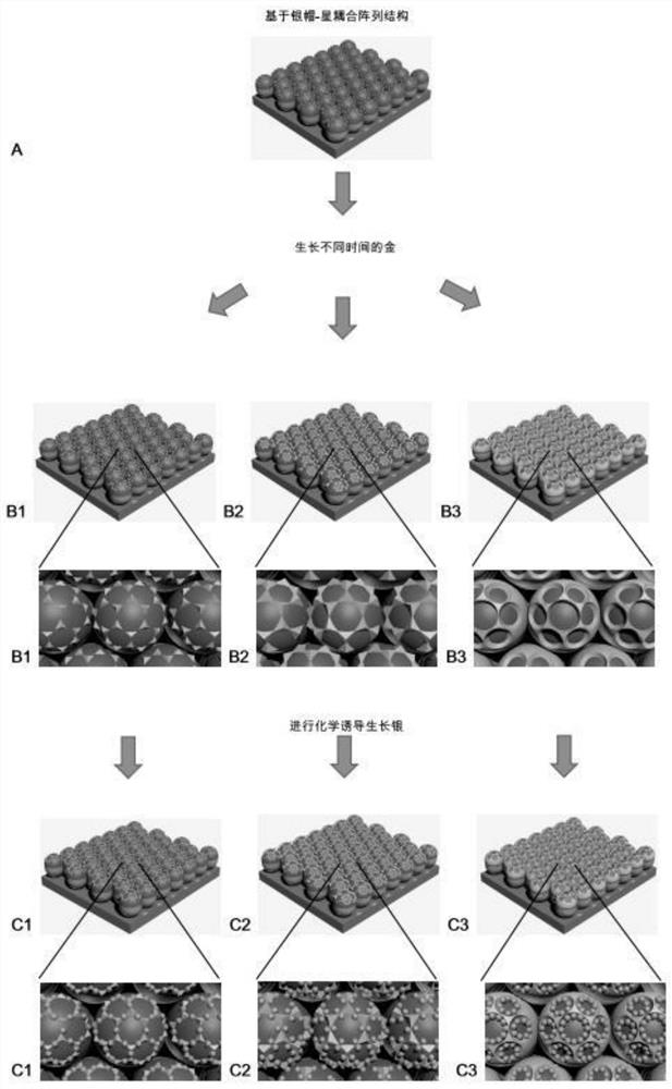
[0050] according to figure 1 The flow chart for preparing the curved honeycomb array precursor is shown:

[0051] (A) On the basis of multilayer nanocap-star coupled periodic array, sputtering Pt to form Pt nanocap-star coupled periodic array structure;

[0052] (B) sputtering a layer of Au with a thickness of 30nm on the basis of the nanocap-star coupled periodic array structure in step (A), to obtain a curved surface honeycomb array precursor (such as figure 1 shown in B1), including Pt-SiO 2 The double-layer substrate and the nano-Au honeycomb array precursor grown on its surface; the SEM image of the structural precursor of the honeycomb structure variant can be found in Figure 8 .

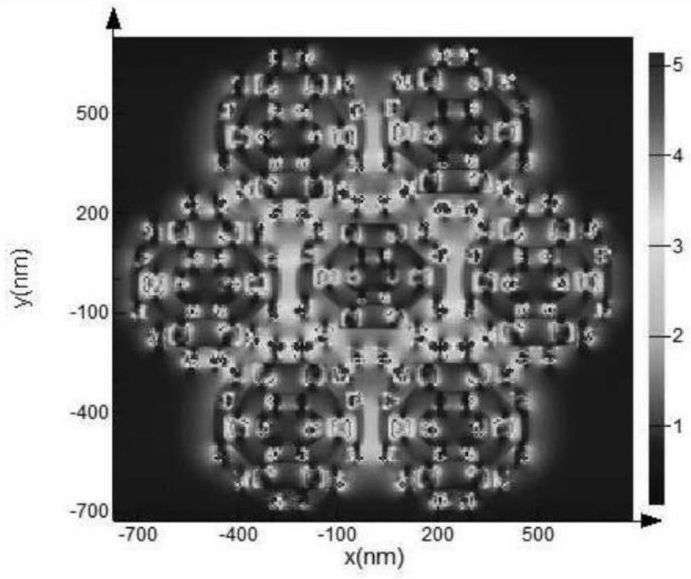
[0053] figure 2 It is the FDTD structure simulation diagram of the curved surface honeycomb array precursor prepared in this embodiment. It can be seen from the figure that the triangular pyramid array attached with nano-gold is attached to the surface of the sphere in the shape of a he...

Embodiment 2

[0056] according to figure 1 The flow chart shown in the preparation of curved surface honeycomb array structure 1:

[0057] (A) On the basis of the multilayer nanocap-star coupled periodic array, Ag sputtered to form the Ag nanocap-star coupled periodic array structure;

[0058] (B) sputtering a layer of Pt with a thickness of 80nm on the basis of the nanocap-star coupling periodic array structure in step (A), to obtain a curved surface honeycomb array structure one (such as figure 1 B2), including Ag-SiO 2 Double-layer substrate and nano-Pt honeycomb array structure grown on its surface; the SEM image of the precursor of the honeycomb structure can be found in Figure 9 .

[0059] Figure 4 It is the FDTD structure simulation diagram of the curved surface honeycomb array structure 1 prepared in this embodiment. It can be seen from the figure that the porous array is attached to the surface of the sphere in a honeycomb shape, and the appropriate height difference between...

Embodiment 3

[0062] according to figure 1 The flow chart shown in the preparation of curved surface honeycomb array structure II:

[0063] (A) On the basis of multilayer nanocap-star coupled periodic array, sputtering Pt to form Pt nanocap-star coupled periodic array structure;

[0064](B) sputtering a layer of Au with a thickness of 120nm on the basis of the nanocap-star coupled periodic array structure in step (A), to obtain a curved surface honeycomb array structure 2 (such as figure 1 B3), including Pt-SiO 2 The double-layer substrate and the nano-Au honeycomb array structure grown on its surface II; the SEM picture of the structural precursor of the honeycomb structure can be found in Figure 9 .

[0065] Figure 6 It is the FDTD structure simulation diagram of the curved honeycomb array structure 2 prepared in this embodiment. It can be seen from the figure that the porous array is attached to the surface of the sphere in a honeycomb shape, and the appropriate height difference b...


PUM

PropertyMeasurementUnit
radiusaaaaaaaaaa
radiusaaaaaaaaaa
diameteraaaaaaaaaa

Abstract

The invention provides a construction method of a curved surface honeycomb array and application of the curved surface honeycomb array, and particularly relates to evolution of two different curved surface honeycomb structures and feasible application in different fields. A solution used for light-operated growth regulation is selected from one of a silver nitrate solution, a tetraammineplatinum dihydroxide solution and a chloroauric acid solution. According to the construction method of the curved surface honeycomb array and application of the curved surface honeycomb array, the structure is further evolved on the basis of the prior art, the operability of the structure is further improved, meanwhile, the production period of an ordered nanostructure active substrate is not long, the cost is low, the test condition requirements are relatively simple, therefore, the construction method of the curved surface honeycomb array and application of the curved surface honeycomb array have the advantages that the uniformity is good, the order degree is high, the repeatability is high, construction steps are simple, the production period is short, and the cost is low, and the operable space of the nanometer ordered structure and the applicable space of the substrate are further enlarged.

Description

technical field [0001] The invention relates to the technical field of nanocomposite materials, in particular to a construction method and curved surface of a curved honeycomb array with high variability, large operable space, wide application range, good uniformity, high degree of order, and strong repeatability Applications of honeycomb arrays. Background technique [0002] Localized surface plasmons have been widely studied and applied in many fields such as Raman scattering, scanning near-field optical microscopy, biosensors, magneto-optical data storage, and optical devices. In recent years, the enhancement of solar cell efficiency by localized surface plasmons has become one of the hotspots in the research and application of localized surface plasmons. Solar energy has great potential to solve the global energy crisis and improve the environment. [0003] At present, the most widely produced and applied solar material is crystalline silicon wafer, with a thickness of...

Claims


Application Information

Patent Timeline
Patent Type & Authority Applications(China)
IPC IPC(8): C23C28/00C23C14/20C23C14/34C23C18/08C23C18/14B82Y40/00G01N21/65G11C11/02G11C11/42
CPCC23C28/322C23C28/345C23C28/3455C23C14/34C23C14/205C23C14/223C23C14/0005C23C18/143C23C18/08B82Y40/00G01N21/658G11C11/02G11C11/42
Inventor 王雅新赵晓宇徐巍温嘉红张永军
Owner HANGZHOU DIANZI UNIV
Why Eureka
Try Eureka