Semiconductor device and manufacturing method thereof

A manufacturing method and semiconductor technology, which are applied in the fields of semiconductor/solid-state device manufacturing, semiconductor devices, semiconductor/solid-state device components, etc., can solve the problems of low efficiency, failure of TSV structure electrical performance, and high cost, and achieve improved electrical stability, The effect of improving the ability of metal diffusion and improving the ability to resist voltage breakdown

Pending Publication Date: 2021-11-09
WUHAN XINXIN SEMICON MFG CO LTD
View PDF7 Cites 0 Cited by
  • Summary
  • Abstract
  • Description
  • Claims
  • Application Information

AI Technical Summary

Problems solved by technology

[0003] However, the use of ALD technology to form a silicon oxide layer is a process with high cost and low efficiency; and the ability of the silicon oxide layer to prevent metal diffusion in the metal layer and prevent voltage breakdown is limited, which can easily lead to electrical failure of the TSV structure

Method used


Image

  • Semiconductor device and manufacturing method thereof
  • Semiconductor device and manufacturing method thereof
  • Semiconductor device and manufacturing method thereof

Examples


Embodiment Construction

[0037] In order to make the purpose, advantages and features of the present invention clearer, the semiconductor device and its manufacturing method proposed by the present invention will be further described in detail below. It should be noted that all the drawings are in a very simplified form and use imprecise scales, and are only used to facilitate and clearly assist the purpose of illustrating the embodiments of the present invention. The meaning of "and / or" in this article is to choose one or both.

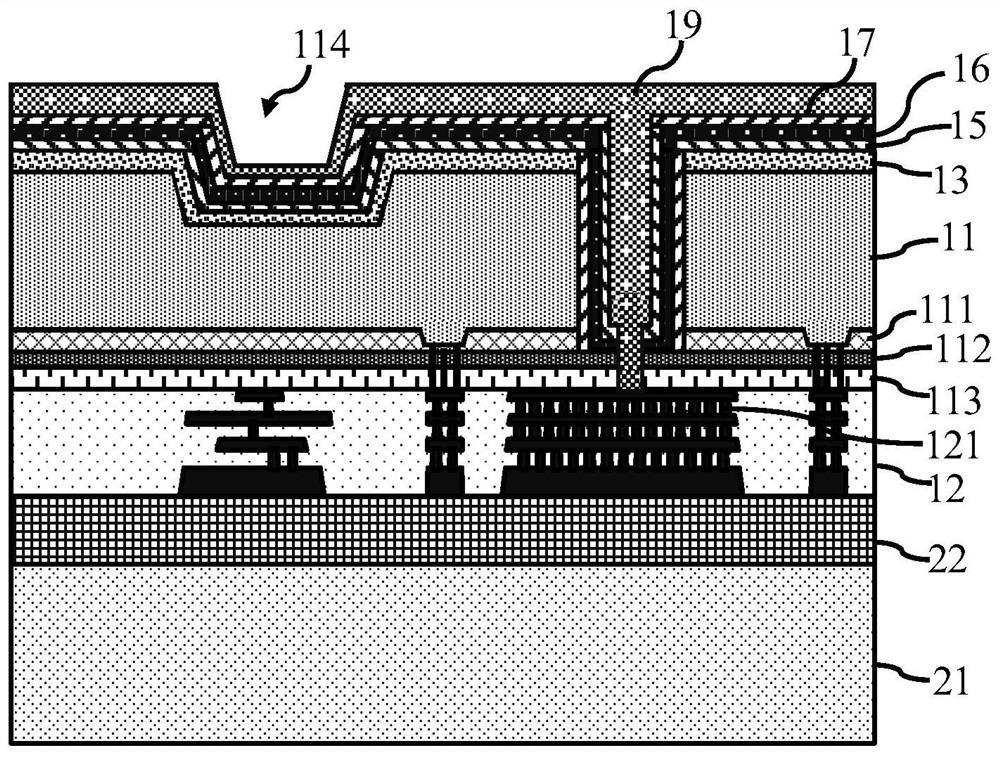
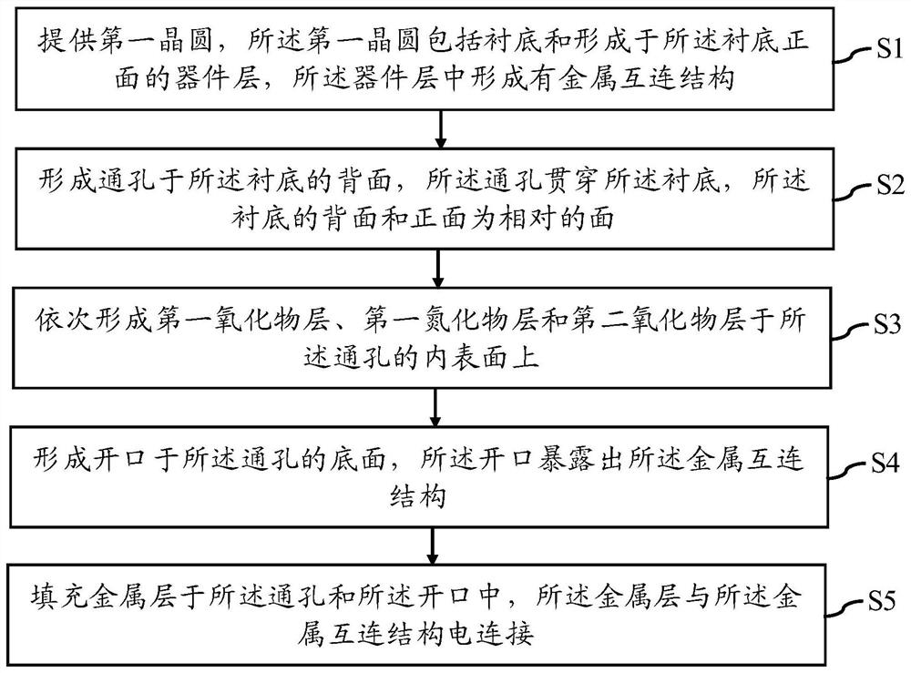
[0038] An embodiment of the present invention provides a semiconductor device, the semiconductor device includes a first wafer, a first oxide layer, a first nitride layer, a second oxide layer and a metal layer, the first wafer includes A substrate and a device layer formed on the front side of the substrate, a metal interconnection structure is formed in the device layer, a through hole is formed on the back side of the substrate, the through hole penetrates the substrate, ...


PUM


Abstract

The invention provides a semiconductor device and a manufacturing method thereof. The semiconductor device comprises a first wafer which comprises a substrate and a device layer formed on the front surface of the substrate, a metal interconnection structure is formed in the device layer, a through hole is formed in the back surface of the substrate, the through hole penetrates through the substrate, and the back surface and the front surface of the substrate are opposite surfaces; a first oxide layer, a first nitride layer and a second oxide layer are sequentially formed on the inner surface of the through hole, an opening is formed in the bottom surface of the through hole, and the metal interconnection structure is exposed out of the opening; and a metal layer is filled in the through hole and the opening, and the metal layer is electrically connected with the metal interconnection structure. According to the technical scheme provided by the invention, the capabilities of preventing metal diffusion and resisting voltage breakdown are improved, so that the electrical stability is improved, and the production cost is reduced.

Description

technical field [0001] The invention relates to the field of semiconductor integrated circuit manufacturing, in particular to a semiconductor device and a manufacturing method thereof. Background technique [0002] After fusion bonding the front side of the pixel wafer to the carrier wafer using BSI (Back-side Illumination, back-illuminated) technology, the TSV (Through Silicon Vias, through-silicon via) hole is made on the back side of the pixel wafer. The metal interconnection structure (including pads) located on the front side of the pixel wafer is led out. The specific steps include: first, etching the substrate on the back of the pixel wafer to form a through hole through the substrate; then, using ALD (Atomic Layer Deposition, atomic layer deposition) technology to form a silicon oxide layer on the side and bottom of the through hole ; Next, etch the silicon oxide layer on the bottom surface of the through hole and the dielectric layer below the silicon oxide layer t...

Claims


Application Information

Patent Timeline
Patent Type & Authority Applications(China)
IPC IPC(8): H01L23/532H01L23/48H01L21/768H01L27/146
CPCH01L23/481H01L21/76898H01L23/485H01L23/50H01L21/76895
Inventor 姚琴占迪刘天建胡胜
Owner WUHAN XINXIN SEMICON MFG CO LTD
Why Eureka
Try Eureka