Manufacturing method of aluminum nitride substrate template

A production method, aluminum nitride technology, applied in semiconductor/solid-state device manufacturing, semiconductor devices, electrical components, etc., can solve problems affecting product growth efficiency, affecting AlN quality, uneven distribution of holes, etc., to improve photoelectric parameters and The effect of chip reliability, low cost and small internal stress

Active Publication Date: 2021-10-22
山西中科潞安紫外光电科技有限公司
View PDF9 Cites 0 Cited by
  • Summary
  • Abstract
  • Description
  • Claims
  • Application Information

AI Technical Summary

Problems solved by technology

However, these methods in the prior art need to be etched in the reaction chamber after being taken out during etching, so that the production efficiency is greatly reduced, the growth efficiency of the product is affected, and the production cost is increased.
Moreover, in the prior art, dry or wet etching is carried out outside the reaction chamber, and the etched holes are unevenly distributed and large in size, which affects the quality of AlN, resulting in certain stress defects.

Method used


Image

  • Manufacturing method of aluminum nitride substrate template
  • Manufacturing method of aluminum nitride substrate template
  • Manufacturing method of aluminum nitride substrate template

Examples


Embodiment Construction

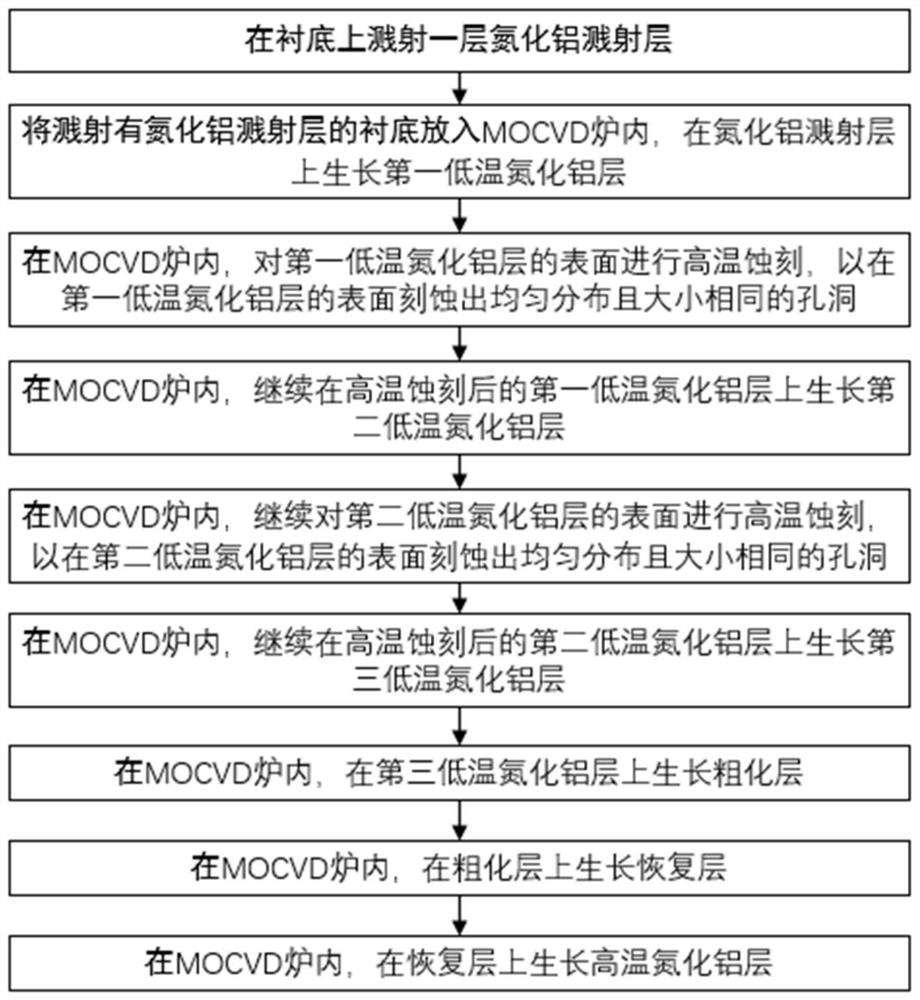
[0037] The present invention will be further described below in conjunction with the accompanying drawings and examples, and the contents of the examples are not intended to limit the protection scope of the present invention.

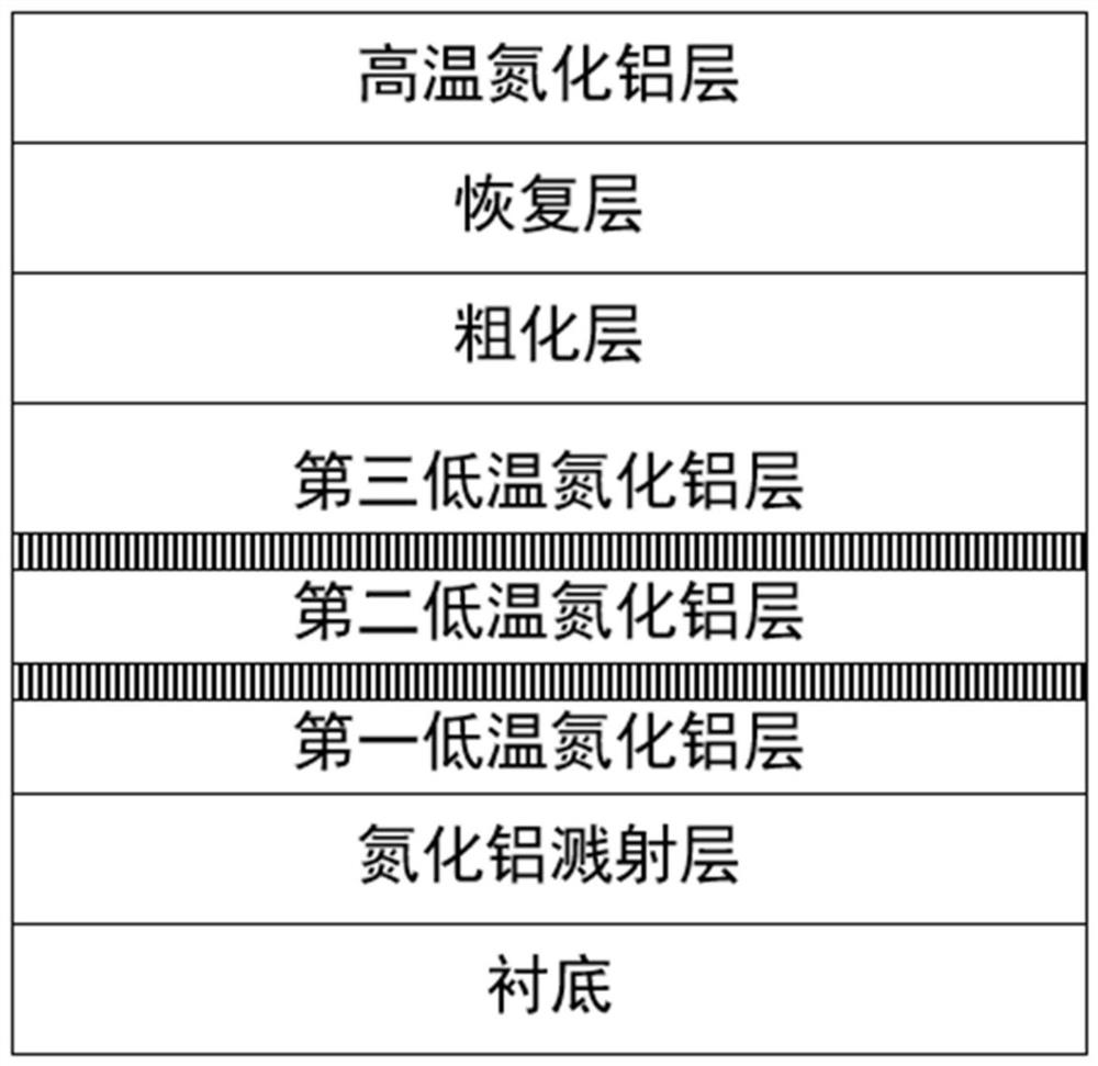
[0038] In order to overcome the problems existing in the prior art, the present invention proposes a method for manufacturing an aluminum nitride substrate template, which etches the low-temperature aluminum nitride layer on the low-temperature aluminum nitride layer through an in-situ high-temperature etching process. Holes with uniform distribution and uniform size can be produced, so as to solve the problem that the internal stress cannot be released due to lattice mismatch during the low-temperature aluminum nitride single crystal epitaxial growth process, and greatly improve the crystal quality of the aluminum nitride layer and the UVC-LED structure , photoelectric performance, reliability, etc.

[0039] figure 1 A flow chart of the manufacturing...


PUM

PropertyMeasurementUnit
thicknessaaaaaaaaaa
thicknessaaaaaaaaaa
thicknessaaaaaaaaaa

Abstract

The invention relates to a manufacturing method of an aluminum nitride substrate template. The manufacturing method comprises the following steps: (1) sputtering an aluminum nitride sputtering layer on a substrate; (2) putting the substrate sputtered with the aluminum nitride sputtering layer into an MOCVD furnace, and growing a first low-temperature aluminum nitride layer on the aluminum nitride sputtering layer; (3) performing high-temperature etching on the surface of the first low-temperature aluminum nitride layer in an MOCVD furnace so as to etch holes which are uniformly distributed and consistent in size in the surface of the first low-temperature aluminum nitride layer; and (4) in the MOCVD furnace, continuously growing a second low-temperature aluminum nitride layer on the first low-temperature aluminum nitride layer after high-temperature etching. According to the invention, cracks on the surface of the aluminum nitride substrate template can be eliminated, various photoelectric parameters and chip reliability of the UVC-LED are improved, the method can be directly carried out in an MOCVD furnace, the manufacturing cost is low, and the method can be applied to large-scale rapid production.

Description

technical field [0001] The invention belongs to the technical field of semiconductor epitaxial substrate growth, and relates to a method for manufacturing an aluminum nitride substrate template. Background technique [0002] AlN templates are more and more widely used in LED materials, especially in the field of deep ultraviolet LED materials. The deep ultraviolet LED materials in the prior art are mainly materials based on AlGaN system. However, there is a serious lattice mismatch problem between the AlGaN material and the substrate, which is prone to defects such as cracks during production. [0003] In order to solve the above problems, a technical solution in the prior art is realized by using an AlN template. The AlN template is a technology that grows AlN on the substrate as a template, so as to re-grow AlGaN materials or similar materials on the template. In this case, the grown AlGaN or similar material layer has strong stability and can not generate cracks under ...

Claims


Application Information

Patent Timeline
Patent Type & Authority Applications(China)
IPC IPC(8): H01L33/00H01L21/02H01L33/20
CPCH01L33/007H01L33/20H01L21/02458H01L21/02513H01L21/0254H01L21/0262Y02P70/50
Inventor 贾晓龙王晓东刘乃鑫闫建昌李晋闽
Owner 山西中科潞安紫外光电科技有限公司
Why Eureka
Try Eureka