Electro-optical device
A technology of electro-optical devices and electrodes, which is applied in the directions of instruments, optics, nonlinear optics, etc., and can solve problems such as electrical crosstalk and frequency band narrowing
- Summary
- Abstract
- Description
- Claims
- Application Information
AI Technical Summary
Problems solved by technology
Method used
Image
Examples
no. 1 approach
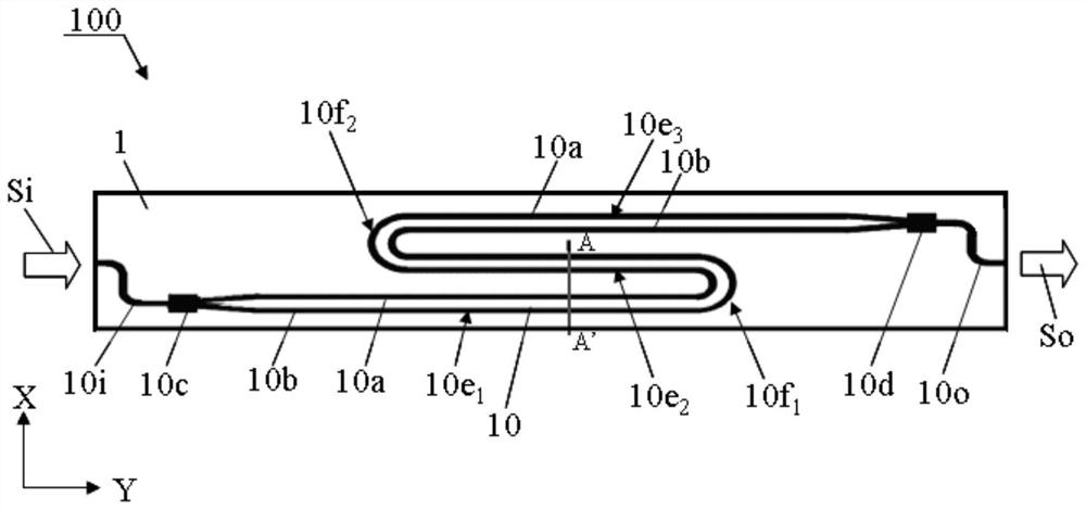
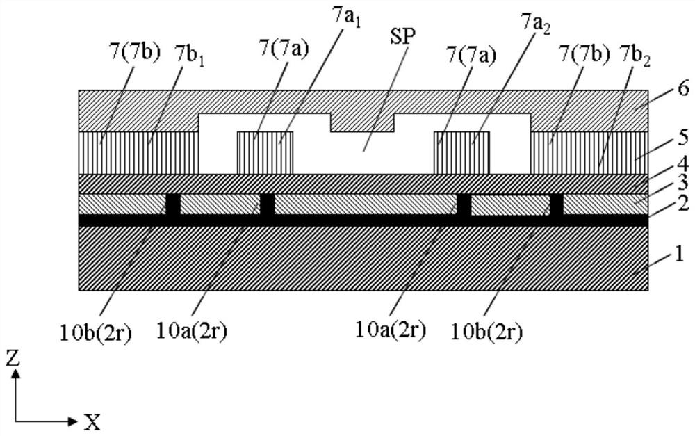
[0036] figure 1 It is a plan view of the optical modulator 100 according to the first embodiment of the present invention. figure 2 is along figure 1 Cross-sectional view of the light modulator at line A-A' in .
[0037] like figure 1 and figure 2 As shown, the optical modulator 100 as the electro-optical device according to this embodiment includes an optical waveguide 10 and an upper electrode 7 arranged on the optical waveguide 10 .
[0038] The optical waveguide 10 is formed by folding back on a plane. For example, in the present embodiment, the optical waveguide 10 is formed by folding back twice on a plane, and includes first to third linear portions 10e arranged in parallel to each other. 1 、10e 2 、10e 3 , connecting the first straight line portion 10e 1 and the second linear portion 10e 2 The first bend 10f 1 , and connecting the second linear portion 10e 2 and the third straight section 10e 3 The second bend 10f 1 . However, the present invention is no...
no. 2 approach
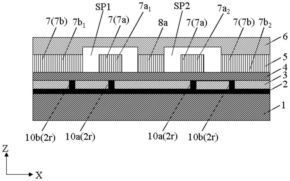
[0058] image 3 is a cross-sectional view of the optical modulator according to the second embodiment of the present invention. like image 3 As shown, the light modulator according to the second embodiment is different from the light modulator 100 according to the first embodiment in that between adjacent parts, that is, from the first adjacent part 7a 1 and the third adjacent portion 7b 1 The group consisting of, and the second adjacent portion 7a 2 and the fourth adjacent portion 7b 2 The ground conductor 8a is arranged between the formed groups. Specifically, as image 3 As shown, in the first adjacent part 7a 1 and the second adjacent portion 7a 2 The ground conductor 8a is arranged between them. Other configurations of the optical modulator according to the present embodiment are the same as those of the optical modulator 100 according to the first embodiment, and thus detailed description thereof will be omitted.
[0059] In addition, in this embodiment, the me...
no. 3 approach
[0067] Figure 7 It is a plan view of the light modulator 200 according to the third embodiment of the present invention. Figure 8 is along Figure 7 Cross-sectional view of the light modulator at line A-A' in . like Figure 7 and Figure 8 As shown, the optical modulator 200 according to this embodiment has four optical waveguides 10 and the first upper electrode 7 a and the second upper electrode 7 b arranged on the optical waveguides 10 . However, the number of optical waveguides 10 is not particularly limited, and there may be 1 to 3 or 5 or more optical waveguides 10 .
[0068] The optical waveguide 10 is a Mach-Zehnder optical waveguide having a first optical waveguide 10a and a second optical waveguide 10b. There are a plurality of first and second optical waveguides 10a, 10b branched from one input optical waveguide 10i by a demultiplexer 10c, and the plurality of first and second optical waveguides 10a, 10b are collected in a plurality of optical waveguides via ...
PUM
| Property | Measurement | Unit |
|---|---|---|
| thickness | aaaaa | aaaaa |
| thickness | aaaaa | aaaaa |
| relative permittivity | aaaaa | aaaaa |
Abstract
Description
Claims
Application Information
 - Generate Ideas
- Intellectual Property
- Life Sciences
- Materials
- Tech Scout
- Unparalleled Data Quality
- Higher Quality Content
- 60% Fewer Hallucinations
Browse by: Latest US Patents, China's latest patents, Technical Efficacy Thesaurus, Application Domain, Technology Topic, Popular Technical Reports.
© 2025 PatSnap. All rights reserved.Legal|Privacy policy|Modern Slavery Act Transparency Statement|Sitemap|About US| Contact US: help@patsnap.com


