
Photosensitive detector based on composite dielectric gate photoconduction and working method thereof

A technology of photosensitive detectors and composite media, applied in semiconductor devices, electric solid devices, circuits, etc., can solve problems such as loss modulation transfer function, image quality constraints, and reduced quantum efficiency, so as to reduce the composite ratio and increase the dynamic The effect of high range and quantum efficiency

Pending Publication Date: 2022-05-13
NANJING UNIV
View PDF1 Cites 0 Cited by
  • Summary
  • Abstract
  • Description
  • Claims
  • Application Information

AI Technical Summary

Problems solved by technology

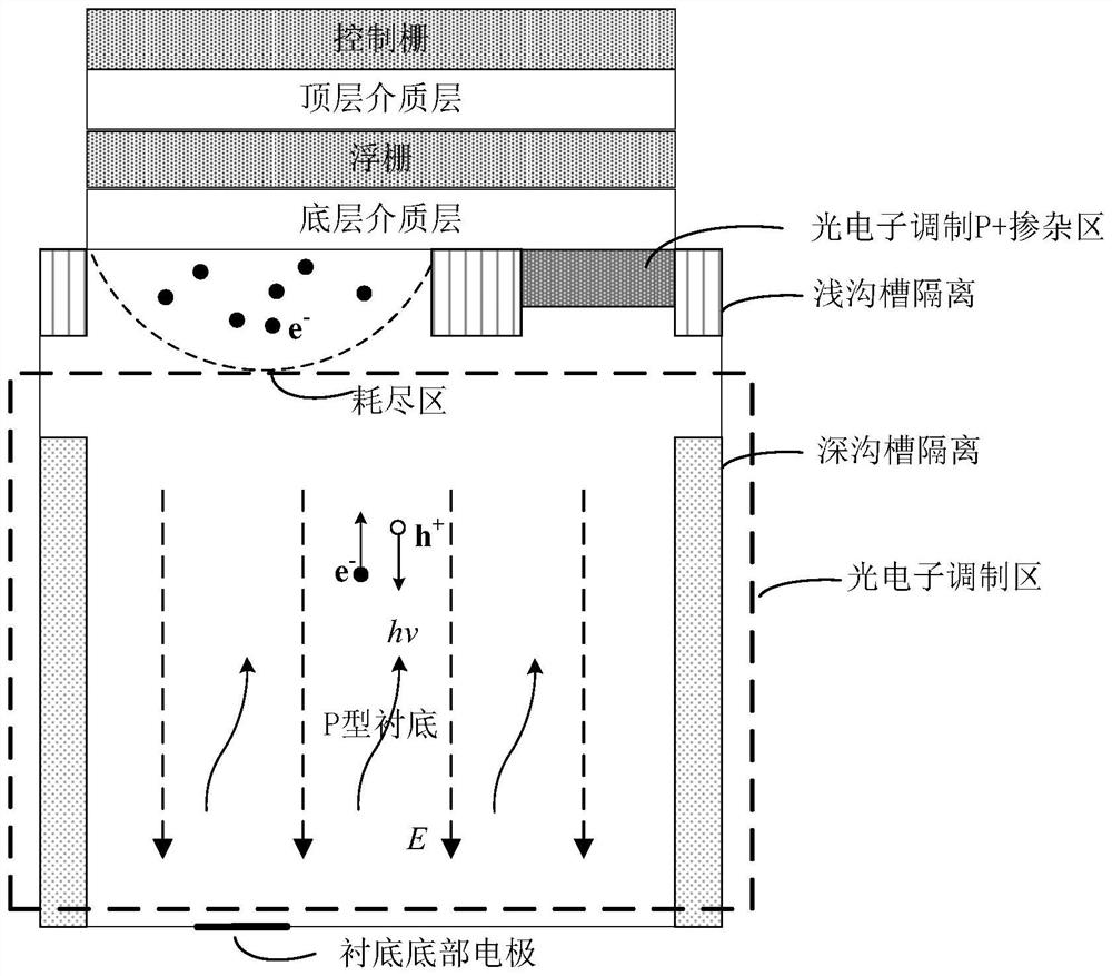
However, due to the large ratio of the detector thickness (above 2um) to the detector size (submicron), the depth of the depletion region under the exposure voltage is difficult to reach 2um, which makes the photogenerated electrons in a part of the body region be directly recombined during exposure. , a part of the photoelectron is lost, which reduces the quantum efficiency, and in the process of electron collection, there is electrical crosstalk, and the modulation transfer function MTF (Modulation Transfer Function, MTF) is lost, and the final image quality is seriously restricted

Method used


Image

  • Photosensitive detector based on composite dielectric gate photoconduction and working method thereof
  • Photosensitive detector based on composite dielectric gate photoconduction and working method thereof
  • Photosensitive detector based on composite dielectric gate photoconduction and working method thereof

Examples


Embodiment Construction

[0034] In order to make the object, technical solution and advantages of the present invention clearer, the embodiments of the present invention will be further described in detail below in conjunction with the accompanying drawings.

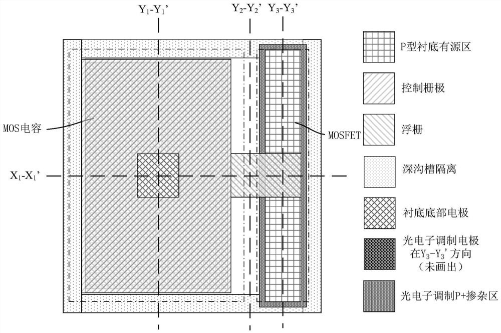
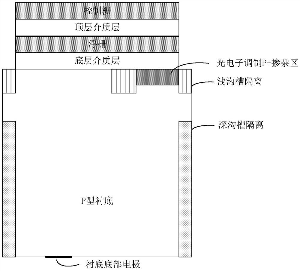
[0035] This embodiment provides a photosensitive detector based on composite dielectric gate photoconductivity that can effectively improve quantum efficiency and suppress electrical crosstalk. It is fabricated on a P-type semiconductor substrate and includes a composite dielectric gate MOS capacitor with photosensitive function. The compound dielectric gate MOSFET part with the function and the optoelectronic modulation structure with the function of improving the quantum efficiency, figure 1 The two-dimensional structure of this photosensitive detector is given, figure 2 , Figure 5 , Figure 7 ~ Figure 9 The structural schematic diagrams of the photosensitive detector along different sections are given respectively.

[0036] Such as fig...


PUM


Abstract

The invention discloses a photosensitive detector based on composite dielectric gate photoconduction and a working method thereof. The photosensitive detector comprises a composite dielectric gate MOS capacitor, a composite dielectric gate MOSFET part and a photoelectron modulation structure which are formed above the same P-type semiconductor substrate, wherein the photoelectron modulation structure comprises a substrate electrode, a photoelectron modulation P + doped region and a photoelectron modulation electrode; the substrate electrode is arranged at the bottom of the P-type semiconductor substrate; an N-type source electrode and a drain electrode are arranged on the surface of the substrate of the composite dielectric gate MOSFET part, and the photoelectron modulation P + doped region is arranged on the periphery of the N-type source electrode and the periphery of the drain electrode; and the photoelectron modulation electrode is positioned on the surface of the photoelectron modulation P + doped region. By controlling the electric field between the bottom of the P-type substrate and the photoelectron modulation P + doped region, photoelectrons in the body region can be collected when the MOS capacitor senses light, and electrical crosstalk between adjacent detectors can be suppressed, so that the quantum efficiency and MTF of the photosensitive detector can be effectively improved.

Description

technical field [0001] The invention relates to an imaging detection device, especially the structure and working mechanism of an imaging detection device in the infrared, visible light band to ultraviolet band, and specifically relates to a photosensitive detector based on a composite dielectric grid photoconductor and its working method. Background technique [0002] The market for solid-state imaging sensors is booming and experiencing exponential growth due to demand in the areas of digital and video cameras, mobile imaging, surveillance and biometrics. Traditionally, CCD is the dominant imaging technology. However, with the rapid development of CMOS technology, CMOS image sensor (CIS) technology has been widely used in many fields, such as PC cameras, mobile phones, high-end digital cameras and other fields. In addition, with the iterative optimization of technology, in Comparable to CCDs in some performance aspects, it has become an alternative to CCDs. However, the ...

Claims


Application Information

Patent Timeline
IPC IPC(8): H01L27/146
CPCH01L27/14665
Inventor 闫锋陈辉沈凡翔王子豪常峻淞胡心怡刘泉朱千琳李张南王凯顾郅扬柴智李龙飞吴永杰吴天泽王一鸣
Owner NANJING UNIV
Learn More