Semiconductor single crystal silicon growth device

A growth device and technology of single crystal silicon, which are applied in the directions of single crystal growth, single crystal growth, crystal growth, etc., can solve the problems of single crystal silicon rod pollution, reduce the conductivity quality, and can not solve the problems of carbon pollution, etc. Reduce rework rate, improve conductive quality, reduce conversion effect

Active Publication Date: 2021-10-01
江苏矽时代材料科技有限公司
View PDF7 Cites 0 Cited by
  • Summary
  • Abstract
  • Description
  • Claims
  • Application Information

AI Technical Summary

Problems solved by technology

During the growth of Czochralski single crystal silicon, the high-temperature quartz cyanide in the single crystal silicon furnace reacts with the graphite heating device to generate SiO and CO. Among them, CO gas is not easy to volatilize, and most of it enters the silicon melt and reacts with molten silicon to produce elemental carbon and CO. SiO, while most of SiO volatilizes from the surface of the melt, and the carbon remains in the molten silicon, and finally enters the crystalline silicon, and the carbon entering the crystalline silicon will pollute the single crystal silicon rod and reduce the conductive quality
[0004] In the prior art, by changing the argon gas outlet of the monocrystalline silicon furnace, the circulating flow path of SiO gas in the furnace is adjusted to reduce the contact range between it and high-temperature graphite components, thereby reducing the generation of CO gas, and achieving a reduction in crystalline silicon The purpose of pollution, but because the high-temperature graphite component is the heat source supply device of the single crystal silicon furnace, due to the diffusivity of the gas, contact with the high-temperature graphite component is inevitable, and the problem of carbon pollution cannot be solved well

Method used


Image

  • Semiconductor single crystal silicon growth device
  • Semiconductor single crystal silicon growth device
  • Semiconductor single crystal silicon growth device

Examples


Embodiment 1

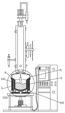
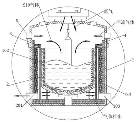
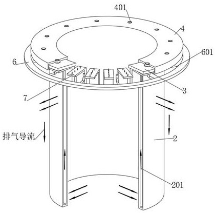
[0044] see Figure 1-10 , a semiconductor single crystal silicon growth device, comprising a single crystal silicon furnace body 1, a graphite heater 101 installed in the single crystal silicon furnace body 1 and a silicon melting crucible 102 matched with the graphite heater 101, the single crystal The silicon furnace body 1 is fixedly installed with a direction-adjusting adsorption cylinder 2 between the graphite heater 101 and the silicon melting crucible 102. The upper end of the direction-adjusting adsorption cylinder 2 is fixedly connected with a microporous one-way adsorption plate 4. An X-type zeolite molecular sieve 3 is fixedly connected to the upper inner wall of the one-way adsorption plate 4, and the inner wall of the X-type zeolite molecular sieve 3 is coated with a layer of cuprous chloride to improve its adsorption capacity for carbon monoxide gas. The microporous one-way adsorption plate 4 The inner wall is connected with an extrusion regeneration assembly 7 m...


PUM


Abstract

The invention discloses a semiconductor single crystal silicon growth device, and belongs to the field of semiconductor manufacturing. The semiconductor single crystal silicon growth device comprises a single crystal silicon furnace body, and a direction adjusting adsorption cylinder located between a graphite heater and a silicon melting crucible is fixedly installed in the single crystal silicon furnace body. An isolation effect can be achieved through the direction adjusting adsorption cylinder, such that the SiO gas cannot approach the graphite heater, and less carbon monoxide is generated. An X-type zeolite molecular sieve, a micro-porous one-way adsorption plate and a reflux gas pump group are matched to perform adsorption circulation on the mixed gas flow on the upper side in the single crystal silicon furnace body. The air flow on the periphery of crystalline silicon is increased while carbon monoxide is effectively removed, convection is formed with introduced argon, the generated carbon monoxide is dispersed and isolated, carbon generation is reduced, and pollution of carbon to the crystalline silicon is reduced. Therefore, the preparation quality of a single crystal silicon rod is improved, the conductive quality of the single crystal silicon rod is improved, the rework rate is reduced, and the economic benefit of manufacturing of the single crystal silicon rod is improved.

Description

technical field [0001] The invention relates to the field of semiconductor manufacturing, more specifically, to a semiconductor single crystal silicon growing device. Background technique [0002] A semiconductor refers to a material whose conductivity at room temperature is between that of a conductor and an insulator. Semiconductor raw materials generally include elements such as silicon, germanium, selenium, and tin oxide, and silicon is the most used element. The semiconductor manufacturing process using silicon as raw material generally includes: polysilicon - zone melting or Czochralski - single crystal silicon rod - rolling, cutting, grinding, polishing - silicon wafer. Among them, the manufacturing process of single crystal silicon rods is also called single crystal silicon growth, and the most commonly used method for single crystal growth is single crystal pulling. [0003] There are many specific processes for pulling single crystals. Commonly used methods inclu...

Claims


Application Information

Patent Timeline
Patent Type & Authority Applications(China)
IPC IPC(8): C30B15/00C30B29/06
CPCC30B15/00C30B29/06
Inventor 徐余琴樊海刚
Owner 江苏矽时代材料科技有限公司
Why Eureka
Try Eureka