Eureka AIR delivers breakthrough ideas for toughest innovation challenges, trusted by R&D personnel around the world.

Diffusion process of solar cell, preparation method of solar cell and silicon wafer

A solar cell and diffusion process technology, applied in the field of solar cells, can solve the problems of increasing open circuit voltage, increasing carrier recombination, affecting doping effect, etc., to achieve the effect of improving conversion efficiency, reducing internal defects, and increasing short-wave response

Pending Publication Date: 2021-09-24
CSG PVTECH +1
View PDF5 Cites 5 Cited by
  • Summary
  • Abstract
  • Description
  • Claims
  • Application Information

AI Technical Summary

Problems solved by technology

[0003] SE technology mainly uses phosphosilicate glass (PSG) as the phosphorus source, and injects the phosphorus source outside the PN junction into the surface layer of the silicon wafer by laser ablation, thereby forming a highly doped region locally, so the diffusion process is used as a laser doping process. The pre-process also provides the necessary phosphorus source for selective doping, but the current diffusion process prepares PN junctions with many redistribution processes of phosphorus sources, which makes the surface concentration of silicon wafers too high and the phosphorus source is unevenly distributed. , to increase carrier recombination, which affects the improvement of solar cell conversion efficiency
[0004] Although the prior art proposes a variety of methods in order to improve the conversion efficiency of solar cells, there are certain defects in these methods.
For example, the prepared PN junction is relatively shallow, and the current paste is generally highly corrosive, so it is easy to be burned through during silk printing and sintering, which affects the performance of the cell; or the residual phosphorus source causes damage to the silicon wafer surface during operation. Damage, and too many oxidation times cause the phosphosilicate glass layer to be too thick, and the concentration difference between the heavily doped region and the lightly doped region is too large to increase the carrier recombination, which is not conducive to improving the open circuit voltage
Or the phosphorus source is deposited too many times, which redistributes the phosphorus source on the surface of the silicon wafer many times, and then makes the overall silicon wafer doping concentration higher, which affects the doping effect and is not conducive to a significant increase in the conversion efficiency of the cell.

Method used


Image

  • Diffusion process of solar cell, preparation method of solar cell and silicon wafer
  • Diffusion process of solar cell, preparation method of solar cell and silicon wafer
  • Diffusion process of solar cell, preparation method of solar cell and silicon wafer

Examples


Embodiment Construction

[0039] The following will clearly and completely describe the technical solutions in the embodiments of the present invention with reference to the accompanying drawings in the embodiments of the present invention. Obviously, the described embodiments are some of the embodiments of the present invention, but not all of them. Based on the embodiments of the present invention, all other embodiments obtained by persons of ordinary skill in the art without making creative efforts belong to the protection scope of the present invention.

[0040] It should be understood that when used in this specification and the appended claims, the terms "comprising" and "comprises" indicate the presence of described features, integers, steps, operations, elements and / or components, but do not exclude one or Presence or addition of multiple other features, integers, steps, operations, elements, components and / or collections thereof.

[0041] It should also be understood that the terminology used ...


PUM


Abstract

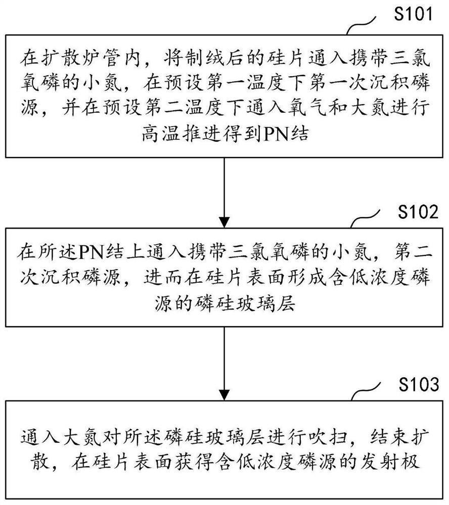
The invention discloses a diffusion process of a solar cell, a preparation method of the solar cell and a silicon wafer, and the diffusion process comprises the steps: introducing small nitrogen carrying phosphorus oxychloride into the textured silicon wafer in a diffusion furnace tube, depositing a phosphorus source at a first temperature, and introducing oxygen and large nitrogen at a second temperature for high-temperature propulsion to obtain a PN junction; introducing small nitrogen carrying phosphorus oxychloride, secondarily depositing a phosphorus source, and further forming a phosphorosilicate glass layer containing a low-concentration phosphorus source on the surface of the silicon wafer; and introducing atmospheric nitrogen to purge, ending diffusion, and obtaining an emitter containing the low-concentration phosphorus source on the surface of the silicon wafer. According to the method, a two-step source deposition mode is adopted, phosphorus oxychloride is deposited in a low-temperature environment, the surface concentration of a silicon wafer can be fully reduced, meanwhile, the uniformity of PN junctions is guaranteed by controlling the gas flow ratio of large nitrogen, oxygen and small nitrogen deposited by a phosphorus source, and the conversion efficiency of a solar cell can be effectively improved.

Description

technical field [0001] The invention relates to the technical field of solar cells, in particular to a diffusion process, a preparation method and a silicon wafer of a solar cell. Background technique [0002] At present, the photovoltaic field is developing rapidly, and photovoltaic products that meet various needs are constantly refreshing the outside world's perception of photovoltaics. How to achieve photovoltaic grid parity is still a topic that is constantly being explored in the photovoltaic field. High-efficiency and low-cost solar cells will gradually become the mainstream of the market. With the continuous update of solar technology, the conversion efficiency of solar cells is also rising. Among emerging technologies, PERC (Passivated Emitter and Rear Cell) batteries with superimposed selective emitter (SE) technology are undoubtedly one of the hottest fields. SE cells can be doped by laser, and have two main features: 1) The contact area between the metal grid l...

Claims


Application Information

Patent Timeline
Patent Type & Authority Applications(China)
IPC IPC(8): H01L31/18H01L21/225H01L31/0288C23C16/34C23C16/40C30B29/06C30B30/00C30B31/08C30B33/00C30B33/02C30B33/10
CPCH01L31/1804H01L31/1864H01L31/0288H01L21/2252C30B31/08C30B30/00C30B29/06C30B33/10C30B33/02C30B33/005C23C16/403C23C16/345Y02P70/50Y02E10/547
Inventor 刘泉陈太昌祁嘉铭陈家健方贵允
Owner CSG PVTECH
Why Eureka
Eureka Blog
Learn More